28
E5400-Pro Series Soft Touch User’s Guide
2
Mechanical Considerations
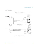
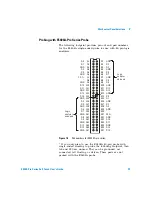
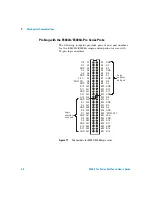
Pin Outs for the Probes
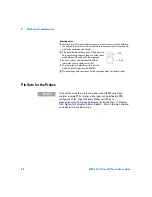
Drawing notes:
1 Maintain a solder mask web between pads when traces are routed between
the pads on the same layer. The solder mask may not encroach onto the pads
within the pad dimension shown.
2 VIAs not allowed on these pads. VIA edges may
be tangent to pad edges as long as a solder mask
web between VIAs and pads is maintained.
3 Surface finishes on pads should be HASL
immersion silver, or gold over nickel.
4 This footprint is compatible with retention
module Agilent model number E5403A.
5 Plated through hole should not be tied to ground plane for thermal relief.
VIA
Pad
N O T E
If you will be using the soft touch probes with a 16900-series logic
analyzer running V2.5 or higher, probe types can be defined in XML
configuration files. To get the latest Probes.xml file, go to
www.agilent.com/find/probe-definitions
. Install the file in c:\Program
Files\Agilent Technologies\AddIns\Agilent\. Refer to the logic analyzer
on-line help for more information.

