background image

26

Getting Started

2.9

AT Power Mode Switch (SW4)

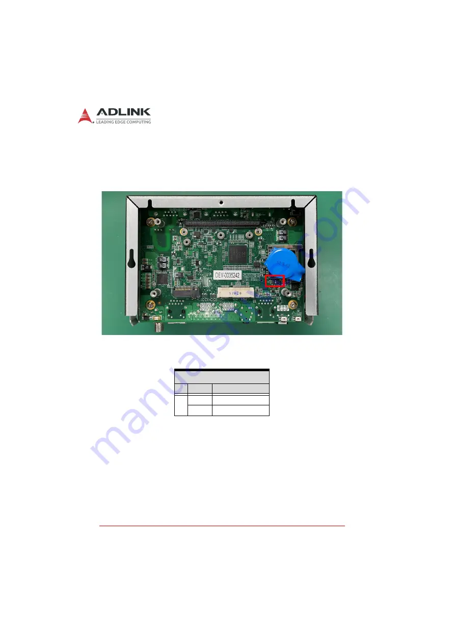
The DLAP-211 is set in AT mode by default. By using the AT
Power Mode Switch (SW4), users can set the system to be pow-
ered-on with the power button.

Figure 2-5: AT Power Mode Switch (SW4)

AT mode can be configured as follows.

Table  2-1: AT Mode Switch Configuration

SW4 Auto Power On

SW4

Auto Power On

2

OFF

Enable (Default)

ON

Disable

Summary of Contents for DLAP-211-JNX Series

Page 1: ...DLAP 211 JNX DLAP 211 JT2 DLAP 211 Nano Series Edge Inference System User s Manual Manual Rev 1 1 Revision Date November 9 2022 Part No 50M 00016 1010 ...

Page 2: ...ii Revision History Revision History Revision Release Date Description of Change s 1 0 2021 12 06 Initial Release 1 1 2022 11 09 Added DLAP 211 JT2 ...

Page 3: ... or documentation even if advised of the possibility of such damages Environmental Responsibility ADLINK is committed to fulfill its social responsibility to global environmental preservation through compliance with the Euro pean Union s Restriction of Hazardous Substances RoHS direc tive and Waste Electrical and Electronic Equipment WEEE directive Environmental protection is a top priority for AD...

Page 4: ...n trying to com plete a task Informations destinées à prévenir les blessures corporelles mineures les dommages aux composants la perte de don nées et ou la corruption de programme lors de l exécution d une tâche WARNING Information to prevent serious physical injury component damage data loss and or program corruption when trying to complete a specific task Informations destinées à prévenir les bl...

Page 5: ... Ethernet GbE Connectors 10 1 5 2 USB 3 0 Connectors 11 1 5 3 12V DC Connector 11 1 5 4 Controller Area Network CAN Bus 12 1 5 5 COM Port 12 1 5 6 HDMI Connectors 13 1 5 7 USB 2 0 OTG Connector 13 1 5 8 D sub 37 pin Connector 14 1 5 9 Side I O Slots 15 2 Getting Started 17 2 1 Unpacking Checklist 17 2 2 Cooling Considerations 17 2 3 Removing the Chassis Cover 18 2 4 Installing an M 2 SSD Module 20...

Page 6: ...er Mode Switch SW4 26 3 Using the System 27 3 1 Software Configuration 27 3 2 System Recovery 27 3 3 COM Port Configuration 29 3 4 SPI I2C and Relay Configuration 30 3 4 1 GPIO 30 3 4 2 SPI I2C Relay 31 Important Safety Instructions 33 Getting Service 37 ...

Page 7: ...SB 3 0 Pin Definition 11 Table 1 7 CAN Bus Pin Definition 12 Table 1 8 RS 232 422 485 Connector Pin Definition 12 Table 1 9 HDMI Connector Pin Definition 13 Table 1 10 USB 2 0 OTG Connector Pin Information 13 Table 1 11 D sub 37 pin Pin Definition 14 Table 2 1 AT Mode Switch Configuration 26 Table 3 1 COM Port Names 29 Table 3 2 DLAP 211 JNXS GPIO Map Table 30 Table 3 3 DLAP 211 JT2S GPIO Map Tabl...

Page 8: ...viii List of Tables This page intentionally left blank ...

Page 9: ...NanoS JT2S NXS Side View 6 Figure 1 5 DLAP 211 NanoS JT2S NXS Front Panel I O Connec tors 1 7 Figure 1 6 DLAP 211 NanoS JT2S NXS Front Panel I O Connec tors 2 7 Figure 1 7 Rear Panel I O Connectors 9 Figure 1 8 USIM SD Side Door 15 Figure 2 1 M 2 2242 B Key Slot 20 Figure 2 2 Mini PCIe Wi Fi Slot 21 Figure 2 3 VESA Mount 24 Figure 2 4 DIN Rail Mount 25 Figure 2 5 AT Power Mode Switch SW4 26 Figure...

Page 10: ...x List of Figures This page intentionally left blank ...

Page 11: ...cing capabilities in a compact size The DLAP 211 also supports reserved AFM connectors for optional I Os including GPIO Relay I2 C and SPI With a lockable HDMI display two GbE ports four USB 3 0 ports plus a USB 2 0 OTG port for soft ware updates one COM port one isolated CAN bus one audio jack plus one M 2 NVME SATA and one SD slot for additional stor age options a Mini PCIe slot and USIM socket ...

Page 12: ... Denver 2 64 bit and 4 core ARM Cortex A57 4 core ARM Cortex A57 RAM 8 16GB 8GB 4GB Storage 16 GB eMMC 5 1 OS Linux Ubuntu Front Panel I O Ports Button 1x power 1x reset 1x recovery HDMI 1x lockable USB 4x USB 3 0 Type A Ethernet 2x 10 100 1000 Mbps Ethernet Audio Mic in Line out Expansion I O N A 2x I2C 2x SPI 1x UART 8x GPIO 1x Relay through 1x D sub 37 pin connector N A 2x I2C 2x SPI 1x UART 8x...

Page 13: ... JT2 Nano 148 x 120 x 64 mm DLAP 211 JNXS JT2S NanoS Weight Gross 1 725 KG Net 1 5 KG Mounting Wall and VESA DIN rail optional SMA Antenna Connector 4 Environmental Operating Temperature 20 C to 70 C system level 20 C to 85 C board level Operating Humidity 95 40 C non condensing Storage Temperature 40 C to 85 C Vibration Operating 5Grms 5 to 500 Hz 3 axes w mSATA Model DLAP 211 JNX DLAP 211 JNXS D...

Page 14: ...8kV Regulatory CE FCC class B EN61000 6 4 6 2 CE LVD UL by CB FCCID DLAP 211 JNXO DLAP 211 NanoO support CE FCC class A with 4V for one camera connected Firmware WDT WDT Supported Model DLAP 211 JNX DLAP 211 JNXS DLAP 211 JT2 DLAP 211 JT2S DLAP 211 NanoS DLAP 211 NanoS Table 1 1 Specifications ...

Page 15: ... 5 DLAP 211 JNX DLAP 211 JT2 DLAP 211 Nano Series 1 3 Mechanical Dimensions All dimensions shown in millimeters mm Figure 1 1 DLAP 211 Nano JT2 NX Front View Figure 1 2 DLAP 211 Nano JT2 NX Side View 148 52 10 105 ...

Page 16: ...6 Introduction Figure 1 3 DLAP 211 NanoS JT2S NXS Front View Figure 1 4 DLAP 211 NanoS JT2S NXS Side View 148 64 105 ...

Page 17: ...1 Nano Series 1 4 External Layout DLAP 211 NanoS JT2S NXS Front Panel Figure 1 5 DLAP 211 NanoS JT2S NXS Front Panel I O Connectors 1 DLAP 211 NanoS JT2S NXS Front Panel Figure 1 6 DLAP 211 NanoS JT2S NXS Front Panel I O Connectors 2 A B C D E D F G ...

Page 18: ...rd shutdown on the system B Recovery button Press this button to force the system into recovery mode See Section 3 2 System Recovery C Reset button The reset button executes a hard reset on the system D GbE connector LAN 1 GbE from NVIDIA Jetson modules See Section 1 5 Pin Definitions D GbE connector LAN 2 GbE from Intel I210 See Section 1 5 Pin Definitions E USB 3 0 See Section 1 5 2 USB 3 0 Conn...

Page 19: ...1 7 Rear Panel I O Connectors Table 1 3 Rear Panel I O Connectors Item Name Description H CAN bus CAN 2 0B backward compatible with 2 0A I Serial port COM port DB 9 connector RS 232 422 485 software programmable J HDMI port HDMI 2 0 with lock K USB 2 0 USB 2 0 OTG Micro USB H I J K ...

Page 20: ...s Table 1 4 NX TX2NX Nano Module I210 LAN LED The following table provides details for the RJ45 GbE pin connec tions Table 1 5 RJ45 GbE Pin Definition Active Link Left LED Speed Right LED 10 Mbps Yellow Blinking N A 100 Mbps Yellow Blinking N A 1000 Mbps Yellow Blinking Green Pin 10BASE T 100BASE TX 1000BASE T 1 TX LAN_TX0 2 TX LAN_TX0 3 RX LAN_TX1 4 LAN_TX2 5 LAN_TX2 6 RX LAN_TX1 7 LAN_TX3 8 LAN_...

Page 21: ...rSpeed Hi Speed Full speed and Low speed USB devices suitable for USB peripherals including USB cameras Table 1 6 USB 3 0 Pin Definition 1 5 3 12V DC Connector The system requires a 12V DC power source with a screw type connector Pin Signal Name 1 USB3 0_P5VA 2 USB2_CMAN 3 USB2_CMAP 4 GND 5 USB3A_CMRXN 6 USB3A_CMRXP 7 GND 8 USB3A_CMTXN 9 USB3A_CMTXP 12V GND ...

Page 22: ...tion Pin Signal Description 1 NC Not connected 2 CAN0_Low Differential CAN signal negative level 3 NC Not connected 4 NC Not connected 5 NC Not connected 6 NC Not connected 7 CAN0_High Differential CAN signal positive level 8 NC Not connected 9 NC Not connected Pin RS 232 RS 422 RS 485 1 DCD COM_TXD_N COM_D 2 COM_RXD COM_TXD_P COM_D 3 COM_TXD COM_RXD_P NC 4 DTR COM_RXD_N NC 5 COM_GND NC NC 6 NC NC...

Page 23: ...B 2 0 OTG Connector Pin Information Pin Signal Pin Signal 1 TMDS Data2 2 TMDS Data2 Shield 3 TMDS Data2 4 TMDS Data1 5 TMDS Data1 Shield 6 TMDS Data1 7 TMDS Data0 8 TMDS Data0 Shield 9 TMDS Data0 10 TMDS Clock 11 TMDS Clock Shield 12 TMDS Clock 13 CEC 14 Reserved 15 SCL 16 SDA 17 DDC CEC Ground 18 5 V Power 19 Hot Plug Detect Pin Signal Description 1 VCC_USBDev USB device power 2 USB_D1_n Universa...

Page 24: ...PI0_MISO 3 3V 9 SPI0_CS0_L 3 3V 10 GND 11 GPO1 GPIO_14 3 3V 12 GPO2 GPIO_12 3 3V 13 GPO3 GPIO_10 3 3V 14 GPO4 GPIO_06 3 3V 15 GPI1 GPIO_05 3 3V 16 GPI2 GPIO_04 3 3V 17 GPI3 GPIO_03 3 3V 18 GPI4 GPIO_02 3 3V 19 GND 20 GND 21 JUMPER2_EN 22 GPIO_07 23 I2C0_SDA 3 3V 24 I2C0_SCL 3 3V 25 GND 26 GND 27 3 3V 28 3 3V 29 GND 30 UART0_RTS 3 3V 31 UART0_CTS 3 3V 32 UART0_TXD 3 3V 33 UART0_RXD 3 3V 34 GND 35 G...

Page 25: ...to install or remove a user provided SD card USIM Slot The DLAP 211 is equipped with a USIM slot connected to the Mini PCIe connector for use with a user provided SIM card and 3G 4G Mini PCIe module to provide cellular communication Install or remove a SIM card module via the side door NOTE NOTE The 3G 4G Mini PCIe module requires a user provided SIM card for communication via a telecom operator S...

Page 26: ...16 Introduction Orientation Insert the SIM and SD cards with the orientations shown below ...

Page 27: ...n from your dealer before returning any product to ADLINK Ensure that the fol lowing items are included in the package DLAP 211 unit Screw pack VESA mount kit plus optional DIN rail kit if applicable 60W Power adapter 2 2 Cooling Considerations All heat generating components of the DLAP 211 are located on the left side of the system These components directly contact the heat sink via thermal pads ...

Page 28: ...LAP 211 s internal components remove the underside of the chassis as follows 1 On the front panel remove the nut and washer from the 12V DC connector and remove the two mounting screws as indicated in the figure below 2 Remove one screw on the underside of the device ...

Page 29: ...ing Started 19 DLAP 211 JNX DLAP 211 JT2 DLAP 211 Nano Series 3 Slide the cover in the direction indicated by the red arrow 4 Lift the cover off of the chassis Reverse the steps to replace the bottom cover ...

Page 30: ...or B M key module into the indi cated slot under the wires at an angle Figure 2 1 M 2 2242 B Key Slot 2 Press down on the M 2 module until it is seated then secure it with one M2 5 P head L5 screw not provided 3 Replace the bottom cover of the chassis CAUTION Take care not to remove or damage any wires while installing the module ...

Page 31: ...t at an angle Figure 2 2 Mini PCIe Wi Fi Slot 2 Press down on the module until it is seated then secure it to the board using two M2 5 P head L5 screws not provided 3 Attach the wires and antennas that came with your Wi Fi kit It is recommended that the Wi Fi antenna be con nected to the left SMA antenna port and Wi Fi blue tooth antennal be connected to the right SMA antenna port 4 Replace the bo...

Page 32: ...he DLAP 211 DC power input connector uses V V and chas sis ground pins WARNING Before providing DC power to the DLAP 211 ensure the volt age and polarity provided are compatible with the DC input Improper input voltage and or polarity can be responsible for system damage Avant de connecter le PC DLAP 211 à une source de courant continu veuillez vous assurer de la polarité de la tension con forméme...

Page 33: ...se V V et châssis broches de terre NOTE NOTE For additional assistance and information contact ADLINK To reduce potential safety hazards use only the AC adapter pro vided with the product a replacement AC adapter provided by ADLINK or an AC adapter purchased as an accessory from ADLINK Si vous avez besoin d aide supplémentaire veuillez contacter ADLINK pour plus d informations Pour réduire les pro...

Page 34: ...the bottom of the chassis 3 Securely attach the device to the VESA bracket by first inserting the heads of the screws into the wider openings of the VESA bracket s mounting holes then sliding the device down such that the screws are now firmly held by the narrower portions of the mounting holes Figure 2 3 VESA Mount NOTE NOTE It is recommended that four M4 screws 6cm in length be used to attach th...

Page 35: ... its own six M4 screws in addition to the standard VESA mount kit Follow these steps to install the DIN rail bracket 1 Use two M4 screws pointing upwards in the red box below to attach the DIN rail bracket to the adapter plate 2 Use four M4 screws circled in red below to attach the DIN rail bracket assembly to the DLAP 211 chassis Figure 2 4 DIN Rail Mount ...

Page 36: ...ault By using the AT Power Mode Switch SW4 users can set the system to be pow ered on with the power button Figure 2 5 AT Power Mode Switch SW4 AT mode can be configured as follows Table 2 1 AT Mode Switch Configuration SW4 Auto Power On SW4 Auto Power On 2 OFF Enable Default ON Disable ...

Page 37: ... https www adlinktech com Products Deep_Learning_Accelerator _Platform_and_Server Inference_Platform DLAP 211 JT2 DLAP 211 Nano https www adlinktech com Products Deep_Learning_Accelerator _Platform_and_Server Inference_Platform DLAP 211 Nano 3 2 System Recovery You will need a Linux host PC Ubuntu is recommended in order to flash your client device with a new system image Complete the following st...

Page 38: ... recognizes the client and you may proceed If not double check the OTG cable connection and perform troubleshooting as needed until the client is recognized Figure 3 1 Successful Client Host Connection 9 Download mfi_jetson xxx xxx ver xxx tbz2 to the host and client systems 10 Run the following commands in the directory that con tains the downloaded files sudo tar xvjf mfi_jetson xxx xxx ver xxx ...

Page 39: ... 3 1 COM Port Names Switching between RS 232 422 485 echo rs232 sys class sp339_mode_ctl uartMode echo rs422 sys class sp339_mode_ctl uartMode echo rs485 sys class sp339_mode_ctl uartMode Checking the current mode of the serial port cat sys class sp339_mode_ctl uartMode Model COM Port Name DLAP 211 JNX JNXS ttyTHS0 DLAP 211 JT2 JT2S ttyTHS2 DLAP 211 Nano NanoS ttyTHS1 ...

Page 40: ...LAP 211 NanoS GPIO map table Table 3 4 DLAP 211 NanoS GPIO Map Table Pin Signal GPIO Number Pin Signal GPIO Number 11 GPO 1 gpio345 15 GPI 1 gpio266 12 GPO 2 gpio268 16 GPI 2 gpio265 13 GPO 3 gpio417 17 GPI 3 gpio264 14 GPO 4 gpio267 18 GPI 4 gpio419 Pin Signal GPIO Number Pin Signal GPIO Number 11 GPO 1 gpio278 15 GPI 1 gpio408 12 GPO 2 gpio338 16 GPI 2 gpio411 13 GPO 3 gpio337 17 GPI 3 gpio410 1...

Page 41: ...nd cat sys class gpio gpio266 value 3 4 2 SPI I2C Relay DLAP 211 JNXS JT2S NanoS SPI I2C Relay map table Table 3 5 DLAP 211 NanoS GPIO Map Table Model I2C Name SPI Name Relay GPIO Number DLAP 211 JNXS i2c1 dev spidev0 0 dev spidev0 1 gpio424 DLAP 211 JT2S i2c2 dev spidev0 0 dev spidev0 1 gpio264 DLAP 211 NanoS i2c3 dev spidev0 0 dev spidev0 1 gpio168 ...

Page 42: ...32 Using the System This page intentionally left blank ...

Page 43: ... the National Electrical Code and NFPA 75 When installing mounting or uninstalling removing the device Turn off power and unplug any power cords cables Reinstall all chassis covers before restoring power To avoid electrical shock and or damage to device Keep device away from water or liquid sources Keep device away from high heat or humidity Keep device properly ventilated do not block or cover ve...

Page 44: ...system up It is recommended that the device be installed only in a server room or computer room where access is Restricted to qualified service personnel or users familiar with restrictions applied to the location reasons therefor and any precautions required Only afforded by the use of a tool or lock and key or other means of security and controlled by the authority responsible for the location C...

Page 45: ... installer l appareil dans Information Salles technologiques conformes à l article 645 du Code national de l électricité et NFPA 75 Lorsque l installation le montage ou la désinstallation le retrait du périphérique est requis Mettez l appareil hors tension et débranchez tous les cordons câbles d alimentation Réinstallez tous les couvercles de châssis avant de rétablir l alimentation Pour éviter le...

Page 46: ...Le cordon d alimentation ou la prise est endommagé e Un liquide a pénétré à l intérieur de l appareil L appareil a été exposé à une forte humidité et ou de la buée L appareil ne fonctionne pas ou ne fonctionne pas selon le manuel de l utilisateur L appareil est tombé et ou a été endommagé et ou présente des signes évidents de dommage Débranchez le cordon d alimentation avant de desserrer les vis à...

Page 47: ...ktech com ADLINK Technology China Co Ltd 300 Fang Chun Rd Zhangjiang Hi Tech Park Pudong New Area Shanghai 201203 China Tel 86 21 5132 8988 Fax 86 21 5132 3588 Email market adlinktech com ADLINK Technology GmbH Hans Thoma Strasse 11 D 68163 Mannheim Germany Tel 49 621 43214 0 Fax 49 621 43214 30 Email emea adlinktech com ADLINK Technology Inc UK Liaison Office First Floor West Exeter House Chiches...

Reviews: