SERIES IP521 INDUSTRIAL I/O PACK EIA/TIA-422B SERIAL COMMUNICATION MODULE
___________________________________________________________________________________________
- 10 -
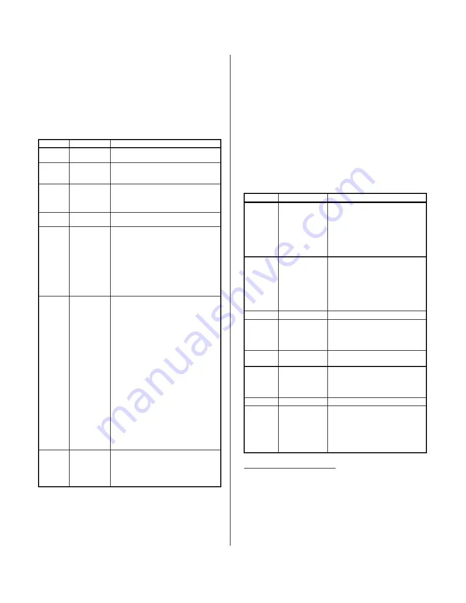
LCR - Line Control Register, Ports A-H (Read/Write)
The Line Control Register is used to specify the asynchronous
data communication format. The word length, the number of stop
bits, and the parity are selected by writing the appropriate bits in this
register.
The individual bits of this register control the format of the data
character as follows:
Line Control Register
LCR Bit
FUNCTION
PROGRAMMING
1,0
Word
Length Sel.
0 0 = 5 Data Bits 0 1 = 6 Data Bits
1 0 = 7 Data Bits 1 1 = 8 Data Bits
2
Stop Bit
Select
0 = 1 Stop Bit
1 = 1.5 Stop Bits if 5 data bits; 2 Stop
Bits if 6, 7, or 8 data bits selected.
3
Parity
Enable
0 = Parity Disabled 1 = Parity Enabled
A parity bit is generated and checked
for between the last data word bit and
the stop bit.
4
Even-Parity
Select
0 = Odd Parity
1 = Even Parity
5
Stick Parity
0 = Disabled, 1 = Enabled
When parity is enabled, stick parity
causes the transmission and reception
of a parity bit to be in the opposite state
from the value selected via bit 4. This
is used as a diagnostic tool to force
parity to a known state and allow the
receiver to check the parity bit in a
known state.
6
Break
Control
0 = Break Disabled, 1 = Break Enabled
When break is enabled, the serial
output line (TxD) is forced to the space
state (low). This bit acts only on the
serial output and does not affect
transmitter logic. For example, if the
following sequence is used, no invalid
characters are transmitted due to the
presence of the break.
1. Load a zero byte in response to the
Transmitter Holding Register
Empty (THRE) status indication.
2. Set the break in response to the
next THRE status indication.
3. Wait for the transmitter to become
idle when the Transmitter Empty
status signal is set high
(TEMT=1); then clear the break
when normal transmission has to
be restored.
7
DLL/DLM
and EFR
Enable Bit
0 = Access Receiver Buffer
1 = Allow Access to Divisor Latches
(DLL & DLM) and Enhanced
Feature Register enabled (EFR).
Note that bit 7 must be set high to access the divisor latch
registers DLL & DLM of the baud rate generator or access the
Enhanced Feature Register (EFR). Bit 7 must be low to access the
Receiver Buffer Register (RBR), the Transmitter Holding Register
(THR), or the Interrupt Enable Register (IER). A power-up or
system reset sets all LCR bits to 0.
A detailed discussion of word length, stop bits, parity, and the
break signal is included in Section 4.0 (Theory of Operation).
MCR - Modem Control Register, Ports A-H (R/W)
The Modem Control register controls the interface with the
modem or data set as described below. For this model, DTR is
used to enable the receiver to enable input of RxD. RTS is used to
enable its corresponding transmitter for output of the TxD signal.
The four modem control inputs (CTS, DSR, DCD, and RI) are
disconnected from their receiver input paths. In addition, the four
modem control outputs (DTR, RTS, OUT1, and OUT2) do not have
transmitter output paths.
Bit-3 of this register must be set to a logic “1” to enable
the corresponding port to issue an interrupt.
Modem Control Register
MCR Bit
FUNCTION
PROGRAMMING
0
Data Terminal
Ready Output
Signal (DTR)
0= DTR* Not Asserted (Inactive)
1= DTR* Asserted (Active)
A DTR signal path is NOT
SUPPORTED by this model.
Instead, this output is used to
enable the receiver of the port
RxD.
1
Ready to Send
Output Signal
(RTS)
0 = RTS* Not Asserted (Inactive)
1 = RTS* Asserted (Active)
A RTS signal path is NOT
SUPPORTED by this model.
Instead, the output is used to
enable the transmitter of the port
TxD.
2
Not Used
No Effect on External Operation
3
Port Interrupt
Disable/Enable
0 = Interrupt Disabled for this
port.
1 = Interrupt Enabled for this
port.
4
Loop-back
1
0 = Loop-back Disabled
1 = Loop-back Enabled
5
2
Xon Control
0 = Disable Xon
1 = Enable any Xon function. In
this mode any RX character
received will enable Xon.
6
2
Not Used
Must be logic 0
7
2
Divide by Four
0 = Divide by one. The crystal
frequency is unchanged.
1 = Divide by four. After the
crystal frequency is divided by 16
it is further divided by 4 (see Table
3.2).
Notes (Modem Control Register):
1. MCR Bit 4 provides a local loopback feature for diagnostic
testing of the UART channel. When set high, the UART serial
output (connected to the TXD driver) is set to the marking
(logic 1 state), and the UART receiver serial data input is
disconnected from the RxD receiver path. The output of the
UART transmitter shift register is then looped back into the
receiver shift register input. The control output (RTS) is
internally connected to the control input DSR (while its
associated pin is forced to its high/inactive state). Thus, in the
loopback diagnostic mode, transmitted data is immediately


