Model DT233-0600
Dual Two-Wire mV/TC Input Transmitters
Acromag, Inc. Tel: 248-295-0880
- 36 -
http://www.acromag.com
- 36 -
https://www.acromag.com
NOTE:
For best accuracy and
performance, mount this unit
upright on a DIN rail and allow
free air flow intake from the
bottom vent to flow through the
unit and out the top vent. This
will allow unit to run cooler,
helping to extend the life of the
electronics. It will also increase
CJC accuracy for TC inputs.
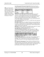
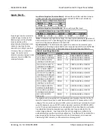
Input Thermocouple CJC Reference (TC Inputs Only):
Table 2 below shows the
accuracy of the CJC sensors used in TB1 and TB3. CJC has been factory calibrated at
25°C to ±0.1°C and its accuracy over the full operating range will be about ±1.0°C.
Table 2: Thermocouple CJC
1
Sensor Absolute Accuracy
CJC Range
Typical
Maximum
25°C
±0.1°C
±0.3°C
10 to 80°C
±0.3°C
±0.6°C
-40 to 80°C
±0.5°C
±1.2°C
1
Note:
Cold Junction Compensation (CJC) may be switched OFF to permit direct
connection of an input millivolt signal via copper wires to simplify calibration.
Otherwise, a hand-held calibrator may be used. For best results, allow the module to
warm-up to thermal equilibrium for 5-10 minutes prior to calibrating CJC. During
calibration, physically position the module the same as its field application
(recommended upright on a DIN rail). Note that the input is normally calibrated with
CJC OFF, and CJC calibration is done separately.
Input Linearization (TC Inputs):
Within
0.25
C of the NIST tables (internal breakpoint
tables resolve to ±0.05°C).
Input Break Detection
: Can be set Upscale or Downscale for open sensor/lead break
fault detection. Output limits are scaled I/O range dependent and can be from 3.5mA
up to 24mA. Unit allows you to set your own output limits, or you may select Namur
Compliant fault limits with a linear operating range from 3.7mA to 20.7mA and break
detect set to levels outside of these limits.
IMPORTANT:
Calibration should be done with break detection already set as required
by the application, as changing it will affect calibration somewhat.
Input Bias Current
: ±125nA typical (TC break current).
Input Analog to Digital Converters (A/D):
Inputs each utilize 24-bit,
-
A/D
converters, with only the first 16-bits used. The A/D signal is then normalized to a
bipolar range count of ±25000 to simplify I/O scaling (see Input Resolution below).
Sampling Rate (A/D):
Inputs sampled at a variable rate with filter as follows:
A/D SAMPLING RATE (SAMPLES/SECOND) PER INPUT FILTER
MODEL
None
Low
Med
High
DT233
107.325sps
26.83125sps
6.71sps
0.83875sps
Input Impedance:
15.4MΩ, typical.
Input Overvoltage Protection:
Inputs include Bipolar Transient Voltage Suppression
(TVS) and diode-clamping along with series resistance and capacitive filtering.
Input Filter:
Normal mode RC filtering, plus digital filtering, optimized and fixed per
filter selection within the
-
ADC. See Normal Mode Noise Rejection & Response
Time.
Input Zero and Full-Scale Adjustment
: Range endpoints are selectable over the full
range noted in Table 1 for each input type. Input Zero and Full-Scale must be within
range and will be mapped to 4mA and 20mA at the output. Input resolution decreases
and potential error magnifies when your programmed input range is reduced.
Nominal rated ±0.1% error assumes a minimum input span of 10mV.


