background image

Chapter    4    Award BIOS Setup


4-3. THE STANDARD CMOS FEATURES


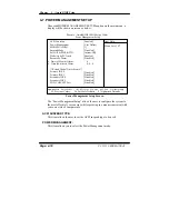
Highlight the

ň

STANDARD CMOS FEATURES

ʼn

and press the <ENTER> 

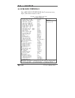
key and the screen will display the following table: 


Phoenix - AwardBIOS CMOS Setup Utility 

Standard CMOS Features 


Date (mm:dd:yy) 
Time (hh:mm:ss) 


ٿ

 IDE Primary Master 

ٿ

 IDE Primary Slave 

ٿ

 IDE Secondary Master 

ٿ

 IDE Secondary Slave 


Drive A 
Drive B 


Video 

Halt On 


Base Memory 
Extended Memory 
Total Memory 


Wed, Jul  14  2004 
10  :  16  :  44 


[None] 
[ST320014A] 
[DV-516E] 
[None] 


[1.44M, 3.5 in.] 
[None] 


[EGA/VGA] 
[All, But Keyboard] 


   640K 
515072K 
516096K 


Item Help 


Menu Level    

Ź


Change the day, month, 
year and century 


npom

:Move    Enter: Select    +/-/PU/PD:Value    F10:Save    ESC:Exit    F1:General Help 

   F5: Previous Values    F6:Fail-Safe Defaults   F7:Optimized Defaults 


CMOS Setup screen


In the above Setup Menu, use the arrow keys to highlight the item and then use 
the <PgUp> or <PgDn> keys to select the value you want in each item. 


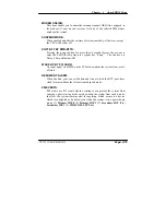
Date:


< Month >, < Date > and <Year >. Ranges for each value are in the CMOS 
Setup Screen, and the week-day will skip automatically. 


Time:


< Hour >, < Minute >, and < Second >. Use 24 hour clock format, i.e., for PM 
numbers, add 12 to the hour. For example: 4: 30 P.M. You should enter the 
time as 16:30:00. 


Page: 4-4 

PC 5151 USER MANUAL


Summary of Contents for PC 5151

Page 1: ...USER S MANUAL PC 5151 Socket 478 P4 P4 M 15 1024X768 Panel PC System Copyright Notice ...

Page 2: ... notice This manual is copyrighted August 2004 You may not reproduce or transmit in any form or by any means electronic or mechanical including photocopying and recording ACKNOWLEDGEMENTS All trademarks and registered trademarks mentioned herein are the property of their respective owners CE NOTICE This is a class A product In a domestic environment this product may cause radio interference in whi...

Page 3: ...h case the user will be required to correct the interference at his own expense You are cautioned that any change or modifications to the equipment not expressly approve by the party responsible for compliance could void your authority to operate such equipment CAUTION Danger of explosion if battery is incorrectly replaced Replace only with the same or equivalent type recommended by the manufactur...

Page 4: ...s Voltage Selection 2 15 2 10 LCD Panel Voltage Selection 2 16 2 11 Power Connector 2 17 2 12 Floppy Disk Drive Connector 2 18 2 13 Hard Disk Drive Connector 2 19 2 14 Printer Connector 2 21 2 15 LAN Connector 2 22 2 16 LAN LED Connector 2 22 2 17 Keyboard Connector 2 23 2 18 PS 2 Mouse Connector 2 23 2 19 Sound Connector 2 24 2 20 Reset Connector 2 25 2 21 HDD LED Connector 2 25 2 22 Power Button...

Page 5: ... 3 7 USB2 0 Chipset Software Installation Utility 3 9 3 8 Touch Screen Driver Utility Optional 3 9 3 9 USB CF Card Driver Utility Optional 3 9 3 10 Watchdog Timer Configuration 3 10 CHAPTER 4 AWARD BIOS SETUP 4 1 Introduction 4 2 4 2 Entering Setup 4 3 4 3 The Standard CMOS Features 4 4 4 4 The Advance BIOS Features 4 8 4 5 The Advanced Chipset Features 4 11 4 6 Integrated Peripherals 4 14 4 7 Pow...

Page 6: ...nel A 8 Exploded Diagram for Removing CD ROM Assembly A 10 Exploded Diagram for Removing HDD Assembly A 11 Exploded Diagram for Removing Motherboard Power A 12 Exploded Diagram for Removing Output Panel A 13 Exploded Diagram for Removing FDD CD ROM A 14 Exploded Diagram for Removing Mask A 16 Exploded Diagram for Wall Mounting A 17 APPENDIX B TECHNICAL SUMMARY Block Diagram B 2 Interrupt Map B 3 R...

Page 7: ...HAPTER 1 This chapter gives you the inform lso outlines the System specifications Section includes z About This Manual z Case Illustration z System Specifications z Safety precautions for a Quick Start ge 2 1 Page 1 1 ...

Page 8: ...The final page of this chapter indicates some safety reminders on how to take care of your system Chapter 2 System Configuration This chapter outlines the components locations and their functions In the end of this chapter you will learn how to set jumper and how to configure the system for your own needs Chapter 3 Software Utilities This chapter contains helpful information for proper installatio...

Page 9: ...Chapter 1 Introduction 1 2 CASE ILLUSTRATION PC 5151 USER MANUAL Page 1 3 ...

Page 10: ... One 184 pin DIMM sockets on board z CACHE Built in CPU 128 256KB Cache z REAL TIME CLOCK CR2023 battery backed CMOS RAM Hardware implementation to indicate century rollover z BIOS Phoenix Award Flash BIOS for plug play function Memory size with 4MB and with VGA BIOS Support S I O Setup z KEYBOARD CONNECTOR Mini DIN connector Supports PC AT Keyboard z MOUSE CONNECTOR Mini DIN connector Supports PS...

Page 11: ...annel LVDS panel 20 pin pin header X 2 on board z WATCHDOG I O port 443H to Enable watchdog I O port 441H to Disable watchdog Selectable for NMI or Reset function Time out timing select 0 8 16 24 32 40 48 56 64 72 80 88 96 104 112 120 sec 25 z IDE INTERFACE Two IDE port support for Ultra ATA 33 66 100 133 Support up to four IDE devices z FLOPPY DISK DRIVE INTERFACE One 26 pin connector Support for...

Page 12: ...r 10 100 1000 mbps Ethernet Support Wake On LAN function z USB CONNECTOR Two USB ports on rear panel One internal USB port for touch panel Complies with USB Spec Rev 2 0 z SOUND RealTek ALC202A AC 97 Codec The signal of MIC in Line in Line out connectors on rear panel and CD audio in designed in as a standard connector z HARDWARE MONITORING FUNCTION Monitor CPU Voltage CPU Temperature and Cooling ...

Page 13: ...y source AU 2 LVDS or similar model z PIXEL PITCH According to the supplier s LCD specification z BRIGHTNESS According to the supplier s LCD specification z CONTRAST RATIO According to the supplier s LCD specification z POWER CONSUMPTION According to the supplier s LCD specification z VIEWING ANGLE According to the supplier s LCD specification z RESPONSE TIME According to the supplier s LCD specif...

Page 14: ... Voltage 5V 5V Wire 5 Wire 7 Wire GENERAL INFORMATION z POWER SUPPLY AC Power 200 watt ATX Power Supply Input Requirement The power supply shall operate from 90 to 132 Vrms or 180 to 264 Vrms The power supply shall operate from an AC mains frequency of 47 through 63Hz The Ac mains single cycle peak inrush current shall be limited to 50 amps cold 80 amps warm measured at 115Vrms 60Hz and coinciding...

Page 15: ... must be connected to supply chassis 3 Voltages and ripple are measured at the load side of mating connectors with a 0 1uF monolithic ceramic capacitor paralleled by a 10uF electrolytic capacitor across the measuring terminals Dimension 80mm x 130mm x 40mm z DRIVE BAYS Optional One 3 5 HDD one slim FDD and one slim CD ROM z EXPANSION SLOTS PCI slot for Riser Card use z CONSTRUCTION Electo Galvaniz...

Page 16: ...o a cold place or vice versa because condensation may come from inside of the system f Place PPC against strong vibrations which may cause hard disk failure g Do not place the system too close to any radio active device Radioactive device may cause interference 3 Handling a Avoid putting heavy objects on top of the system b Do not turn the system upside down This may cause the floppy drive and har...

Page 17: ...ful information that describes the jumper connecto settings and component locations Section includes z Jumper Connector Quick Reference Table z Component Locations z Configuration and Jumper settings z Connector Pin Assignments Page 2 1 ...

Page 18: ...B1 PS 2 Mouse Connector MS1 Sound Connector LINE1 MIC1 SPK1 CDIN1 Reset Connector JP10 9 10 HDD LED Connector HDLED1 Power Button PWBN External SMI Connector JP10 5 7 External Speaker Connector JP10 2 4 6 8 Keylock Connector JP10 1 3 CMOS Function Selection JP4 USB Connector USB1 USB2 USB3 USB4 Reset NMI Clear Watchdog Selection JP6 CPU FAN Connector CPUFAN System FAN Connector SYSFAN North Chip F...

Page 19: ...Chapter 2 Hardware Configuration 2 2 COMPONENT LOCATIONS PC 5151 Connector Jumper and Component locations PC 5151 USER S MANUAL Page 2 3 ...

Page 20: ... pins The jumper can be combined into sets that called jumper blocks When the jumpers are all in the block you have to put them together to set up the hardware configuration The figure below shows how this looks like JUMPERS AND CAPS If a jumper has three pins for example labelled PIN1 PIN2 and PIN3 You can connect PIN1 PIN2 to create one setting and shorting You can either connect PIN2 PIN3 to cr...

Page 21: ...Chapter 2 Hardware Configuration JUMPER DIAGRAMS JUMPER SETTINGS PC 5151 USER S MANUAL Page 2 5 ...

Page 22: ...OM1 COM1 Connector The COM1 Connector assignments are as follows PIN ASSIGNMENT 1 NDCDA 2 NSINA 3 NSOUTA 4 NDTRA 5 GND 6 NDSRA 7 NRTSA 8 NCTSA 9 RIN1 COM1 COM2 COM2 Connector The COM2 Connector assignments are as follows PIN ASSIGNMENT RS 232 RS 422 RS 485 1 NDCDB TX TX 2 NSINB TX TX 3 NSOUTB RX RX 4 NDTRB RX RX 5 GND GND GND 6 NDSRB RTS NC 7 NRTSB RTS NC 8 NCTSB CTS NC 9 RIN2 CTS NC COM2 Page 2 6...

Page 23: ...TRC 5 GND 6 NDSRC 7 NRTSC 8 NCTSC 9 RIN3 COM4 COM4 Connector The pin assignments are as follows PIN ASSIGNMENT 1 NDCDD 2 NSIND 3 NSOUTD 4 NDTRD 5 GND 6 NDSRD 7 NRTSD 8 NCTSD 9 RIN4 All COM port s pin 9 is selectable for RI 5V or 12V For more information please refer to our COM RI and Voltage Selection PC 5151 USER S MANUAL Page 2 7 ...

Page 24: ...2 5 COM PORT RI VOLTAGE SELECTION JP8 COM1 COM2 COM3 and COM4 RI Voltage Selection The selections are as follows SELECTION JUMPER SETTING Pin Closed RI 13 14 JUMPER ILLUSTRATION COM1 Max 1A 5V 3 5 12V 1 3 Page 2 8 PC 5151 USER S MANUAL ...

Page 25: ...Chapter 2 Hardware Configuration RI 15 16 COM2 Max 1A 5V 4 6 12V 2 4 PC 5151 USER S MANUAL Page 2 9 ...

Page 26: ...Chapter 2 Hardware Configuration RI 17 18 COM3 Max 1A 5V 7 9 12V 9 11 Page 2 10 PC 5151 USER S MANUAL ...

Page 27: ...Chapter 2 Hardware Configuration RI 19 20 COM4 Max 1A 5V 8 10 12V 10 12 PC 5151 USER S MANUAL Page 2 11 ...

Page 28: ...lectable for RS 232 422 485 function The jumper settings are as follows COM 2 FUNCTION JUMPER SETTING pin closed JUMPER ILLUSTRATION RS 232 Open RS 422 RS 485 1 2 5 6 7 8 9 10 11 12 13 14 15 16 17 18 19 20 1 3 4 6 7 8 9 10 11 12 13 14 15 16 17 18 19 20 Manufactory default RS 232 Page 2 12 PC 5151 USER S MANUAL ...

Page 29: ...TOR VGA VGA Connector The pin assignments are as follows PIN ASSIGNMENT 1 VGA_RED 2 VGA_GREEN 3 VGA_BLUE 4 NC 5 GND 6 GND 7 GND 8 GND 9 VCC Max 1A 10 GND 11 NC 12 VGA_VDDA 13 VGA_HSYNC_5V 14 VGA_VSYNC_5V 15 VGA_VDDCLK PC 5151 USER S MANUAL Page 2 13 ...

Page 30: ... GND 4 JA3P 15 JA0P 5 JA2M 16 GND 6 JA3M 17 JA0M 7 GND 18 LPVDD 8 GND 19 GND 9 JA1P 20 LPVDD 10 JCLK1P 11 JA1M LVDS2 LVDS Connector The pin assignments are as follows PIN ASSIGNMEN T PIN ASSIGNMENT 1 GND 12 JCLK2M 2 GND 13 GND 3 JA6P 14 GND 4 JA7P 15 JA4P 5 JA6M 16 GND 6 JA7M 17 JA4M 7 GND 18 LPVDD 8 GND 19 GND 9 JA5P 20 LPVDD 10 JCLK2P 11 JA5M Page 2 14 PC 5151 USER S MANUAL ...

Page 31: ...2 9 BRIGHTNESS VOLTAGE SELECTION JP11 Brightness Voltage Selection The selections are as follows SELECTION JUMPER SETTING Pin Closed 5V 3 4 2 5V 1 2 JUMPER ILLUSTRATION Manufacturing Default is set as 5V PC 5151 USER S MANUAL Page 2 15 ...

Page 32: ...are Configuration 2 10 LCD PANEL VOLTAGE SELECTION JP3 LCD Panel Voltage Selection The selections are as follows SELECTION JUMPER SETTING Pin Closed 3 3V 2 3 5V 1 2 JUMPER ILLUSTRATION Page 2 16 PC 5151 USER S MANUAL ...

Page 33: ...R ATX1 Power Connector The pin assignments are as follows PIN ASSIGNMENT 1 VCC3_3 2 VCC3_3 3 GND 4 VCC 5 GND 6 VCC 7 GND 8 NC 9 5VSB 10 VCC12 11 VCC3_3 12 VCC12J 13 GND 14 PS_ON 15 GND 16 GND 17 GND 18 VCC5J 19 VCC 20 VCC PC 5151 USER S MANUAL Page 2 17 ...

Page 34: ...nnector The pin assignments are as follows PIN ASSIGNMENT PIN ASSIGNMENT 1 VCC 2 INDEXJ 3 VCC 4 DSAJ 5 VCC 6 DSKCHGJ 7 NC 8 NC 9 NC 10 MOAJ 11 NC 12 DIRJ 13 RWCJ 14 STEPJ 15 NC 16 WDJ 17 GND 18 WEJ 19 GND 20 TRAK0J 21 GND 22 WPJ 23 GND 24 RDATAJ 25 GND 26 HEADJ Page 2 18 PC 5151 USER S MANUAL ...

Page 35: ...1 IDERSTJ 2 GND 3 PDD7 4 PDD8 5 PDD6 6 PDD9 7 PDD5 8 PDD10 9 PDD4 10 PDD11 11 PDD3 12 PDD12 13 PDD2 14 PDD13 15 PDD1 16 PDD14 17 PDD0 18 PDD15 19 GND 20 NC 21 PDREQ 22 GND 23 PDIOWJ 24 GND 25 PDIORJ 26 GND 27 PIORDY 28 GND 29 PDDACKJ 30 GND 31 IRQ14S 32 NC 33 PDA1 34 P66DET 35 PDA0 36 PDA2 37 PDCSJ1 38 PDCSJ3 39 IDEACTPJ 40 GND PC 5151 USER S MANUAL Page 2 19 ...

Page 36: ... SDD6 6 SDD9 7 SDD5 8 SDD10 9 SDD4 10 SDD11 11 SDD3 12 SDD12 13 SDD2 14 SDD13 15 SDD1 16 SDD14 17 SDD0 18 SDD15 19 GND 20 NC 21 SDREQJ 22 GND 23 SIOWJ 24 GND 25 SIORJ 26 GND 27 SDIORJ 28 PULL LOW 29 SDDACKJ 30 GND 31 IRQ15S 32 NC 33 SDA1 34 S66 DET 35 SDA0 36 SDA2 37 SDCSJ1 38 SDCSJ3 39 IDEACTSJ 40 GND 41 VCC 42 VCC 43 GND 44 NC Page 2 20 PC 5151 USER S MANUAL ...

Page 37: ...connect both DB25 connector and parallel port The pin assignments are as follows LPT1 PIN ASSIGNMENT PIN ASSIGNMENT 1 STBJR 14 AFDJ 2 PD0R 15 ERRJ 3 PD1R 16 PAR_INITJ 4 PD2R 17 SLINJ 5 PD3R 18 GND 6 PD4R 19 GND 7 PD5R 20 GND 8 PD6R 21 GND 9 PD7R 22 GND 10 ACKJ 23 GND 11 BUSY 24 GND 12 PE 25 GND 13 SLCT PC 5151 USER S MANUAL Page 2 21 ...

Page 38: ... is as follows PIN ASSIGNMENT 1 TXD0P 2 TXD0N 3 TXD1P 4 TXD2P 5 TXD2N 6 TXD1N 7 TXD3P 8 TXD3N 9 GND 10 GND 11 NC 12 NC 2 16 LAN LED CONNECTOR LANLED1 LAN LED Connector The pin assignment is as follows PIN ASSIGNMENT 1 SPEED100J 2 SPEED1000J 3 LILEDJ 4 ACTLEDJ Page 2 22 PC 5151 USER S MANUAL ...

Page 39: ...ignments are as follows PIN ASSIGNMENT 1 KB DATA 6 5 2 NC 4 3 3 GND 1 2 4 VCC Max 1A 5 KB CLK 6 NC KB1 2 18 PS 2 MOUSE CONNECTOR MS1 PS 2 Mouse Connector The pin assignments are as follows PIN ASSIGNMENT 1 MS DATA 5 6 2 NC 4 3 3 GND 2 1 4 VCC Max 1A 5 MS CLK 6 NC MS1 PC 5151 USER S MANUAL Page 2 23 ...

Page 40: ...d CDIN connector LINE1 Line In Connector The pin assignment is as follows PIN ASSIGNMENT 1 GND 2 LINE_L 3 LINE_R MIC1 Microphone Connector The pin assignment is as follows PIN ASSIGNMENT 1 GND 2 MIC IN 3 MIC VDD SPK1 Line Out Connector The pin assignment is as follows PIN ASSIGNMENT 1 GND 2 Line Out L 3 Line Out R Page 2 24 PC 5151 USER S MANUAL ...

Page 41: ...N ASSIGNMENT 1 CD L 2 GND 3 GND 4 CD R 2 20 RESET CONNECTOR JP10 9 10 Reset Connector The pin assignment is as follows PIN ASSIGNMENT 9 GND 10 RSTSW 2 21 HDD LED CONNECTOR HDLED1 HDD LED Connector The pin assignment is as follows PIN ASSIGNMENT 1 VCC 2 HD_LED PC 5151 USER S MANUAL Page 2 25 ...

Page 42: ...W_BN1 2 PANSWIN 2 23 EXTERNAL SMI CONNECTOR JP10 5 7 External SMI Connector The pin assignments are as follows PIN ASSIGNMENT 5 P_ESMI 7 GND 2 24 EXTERNAL SPEAKER CONNECTOR JP10 2 4 6 8 External Speaker Connector The pin assignments are as follows PIN ASSIGNMENT 2 VCC 4 P_SPK 6 P_SPK 8 P_SPK Page 2 26 PC 5151 USER S MANUAL ...

Page 43: ... CMOS Function Selection The selections are as follows FUNCTION JUMPER SETTING pin closed JUMPER ILLUSTRATION NORMAL 1 2 CLEAR CMOS 2 3 Manufacturing Default Normal To clear CMOS data user must power off the computer and set the jumper to Clear CMOS as illustrated above After five to six seconds set the jumper back to Normal and power on the computer PC 5151 USER S MANUAL Page 2 27 ...

Page 44: ...ENT 1 USBV0 Max 500mA 2 USBP0N 3 USBP0P 4 GND USB2 Universal Serial Bus Connector The pin assignments are as follows PIN ASSIGNMENT 1 USBV1 Max 500mA 2 USBP1N 3 USBP1P 4 GND USB3 Universal Serial Bus Connector The pin assignments are as follows PIN ASSIGNMENT 1 NC 2 NC 3 NC 4 NC 5 USBV2 Max 500mA 6 USBP2N 7 USBP2P 8 GND Page 2 28 PC 5151 USER S MANUAL ...

Page 45: ... touch panel The pin assignments are as follows PIN ASSIGNMENT 1 USBV4 2 USB_DDT4 3 USB_DDT4 4 GND 2 28 INVERTER CONNECTOR CN2 Inverter Connector The pin assignments are as follows PIN ASSIGNMENT 1 V12SAFE 2 GND 3 BRCRT 4 NC 5 V5SAFE 6 GND 7 LINE OUT R 8 GND 9 LINE OUT L PC 5151 USER S MANUAL Page 2 29 ...

Page 46: ...ER ILLUSTRATION Manufacturing Default is set as Reset User may select to use the Reset or NMI watchdog NMI also known as Non Maskable Interrupt is used for serious conditions that demand the processor s immediate attention it cannot be ignored by the system unless it is shut off specifically To clear NMI command user should short the Clear Watchdog pin via push button Page 2 30 PC 5151 USER S MANU...

Page 47: ...1 GND 2 VCC12 Max 1A 3 FANIO1 2 31 SYSTEM FAN CONNECTOR SYSFAN System Fan Connector The pin assignments are as follows PIN ASSIGNMENT 1 VCC12 Max 1A 2 GND 3 VCC12 Max 1A 2 32 NORTH CHIP FAN CONNECTOR NB_FAN North Chip Fan Connector The pin assignments are as follows PIN ASSIGNMENT 1 VCC Max 1A 2 GND PC 5151 USER S MANUAL Page 2 31 ...

Page 48: ...nnector The pin assignments are as follows PIN ASSIGNMENT 1 3 3V 2 GND 2 34 MEMORY INSTALLATION This system is enhanced with 1 DDR DRAM banks which support up to 1G DRAM BANK CONFIGURATION DIMM 1 TOTAL MEMORY 128M 128MB 256M 256MB 512M 512MB 1G 1G Page 2 32 PC 5151 USER S MANUAL ...

Page 49: ... CPU Selection The selections are as follows FUNCTION JUMPER SETTING P4 M 1 2 P4 Default Open JUMPER ILLUSTRATION Please be aware that when using Pentium 4 M CPU JP1 jumper must set as closed otherwise the P4 M CPU will be damaged vice versa PC 5151 USER S MANUAL Page 2 33 ...

Page 50: ...T 1 DIN0 14 DOUT5 2 DIN1 15 DOUT6 3 DIN2 16 DOUT7 4 DIN3 17 GND 5 DIN4 18 GND 6 DIN5 19 GND 7 DIN6 20 GND 8 DIN7 21 GND 9 DOUT0 22 GND 10 DOUT1 23 GND 11 DOUT2 24 GND 12 DOUT3 25 GND 13 DOUT4 26 GND 2 37 ATX 12V POWER CONNECTOR CN1 ATX 12V Power Connector The pin assignments are as follows PIN ASSIGNMENT 1 GND 2 GND 3 12V 4 12V Page 2 34 PC 5151 USER S MANUAL ...

Page 51: ... Panel Resolution Selection The selections are as follows FUNCTION JUMPER SETTING pin closed Hardware Setting 800 x 600 1 2 Hardware Setting 1024 x 768 3 4 JUMPER ILLUSTRATION Hardware Setting Software Setting default 1280 x 1024 5 6 1024 x 768 7 8 PC 5151 USER S MANUAL Page 2 35 ...

Page 52: ...h BIOS update It also describes how to install the watchdog timer configuration Section includes z Introduction z VGA Driver Utility z Flash BIOS Update z LAN Driver Utility z Sound Driver Utility z Intel Chipset Software Installation Utility z USB2 0 Chipset Software Installation Utility z Touch screen Driver Utility Optional z USB CF CARD Driver Utility Optional z Watchdog Timer Configuration Pa...

Page 53: ... For VGA driver installation D AWDFLASH For BIOS update utility D LAN Intel 82541GI For LAN Driver installation D SOUND Realtel ALC202A AC97 For Sound driver installation D UTILITY Intel Chipset Software Installation Utility For Win 98SE ME 2000 XP D USB 2 0 USB 2 0 Software Installation Utility For Win 98SE 2000 ME XP D Touch Screen Drv For Liyi Touch screen driver For Fujitsu Touch screen driver...

Page 54: ...lation of VGA Driver To install the VGA Driver simply follow the following steps 1 Place insert the Utility Disk into Floppy Disk Drive A B or CD ROM drive 2 Under Windows 9X NT4 0 2000 XP system go to the directory where VGA driver is located 3 Click Setup file for VGA driver installation 4 Follow the instructions on the screen to complete the installation 5 Once installation is completed shut do...

Page 55: ...nufacturer When you get these two files ready follow the following steps for updating your VGA BIOS 1 Install Awdflash exe from Utility Disk to Drive C 2 Insert the VGA BIOS file you have obtained from the vendor Type the path to Awdflash exe and execute the VGA BIOS update with file H15bxxxx bin 3 C UTIL AWDFLASH AWDFLASH H15bxxxx bin 4 The screen will display as the table fount on the next page ...

Page 56: ...the BIOS do not turn off or reset the system or you will damage the BIOS After you have completed all the programming the screen displays the table below FLASH MEMORY WRITER v8 XX C Award Software 2001 All Rights Reserved Flash Type SST 49LF004A 3 3V File Name to Program H20bxxxx bin Checksum XXXXX Reset System or Power off to accomplish update process F1 Reset F10 Exit Please reset or power off t...

Page 57: ...pport various network adapters Installation programs for LAN drivers are listed as follows 1 Win 2000 XP program 2 Win NT4 0 program 3 Linux 4 Netware program 5 Open Server 5 05 6 Unixware 7 x For more details on Installation procedure please refer to Readme txt file found on LAN DRIVER UTILITY Page 3 6 PC 5151 USER S MANUAL ...

Page 58: ...8 program 2 Win 98SE program 3 Win NT 4 0 program 4 Win 2000 program 5 Win ME program 6 Win XP program 3 5 2 Installation Procedure for Windows 9x NT 2000 XP 1 From the task bar click on Start and then Run 2 In the Run dialog box type D Sound setup where D Sound pathname refers to the full path to the source files 3 Click on the OK button or press the ENTER key 4 Click on the Next and OK prompts a...

Page 59: ...nents in Device Manager 3 6 2 Installation of Utility for Windows 98SE ME 2000 XP The Utility Pack is to be installed only for Windows 98SE Windows ME Windows 2000 and XP program It should be installed right after the OS installation kindly follow the following steps 1 Place insert the Utility Disk into Floppy Disk Drive A B or CD ROM drive 2 Under Windows 98SE ME 2000 XP system go to the director...

Page 60: ...n 5 Double Click USB Root Hub 6 Select Driver 7 Click Install to install the driver 8 Follow the instructions on the screen to complete the installation 9 Click Finish after the driver installation is complete 3 8 TOUCH SCREEN DRIVER UTILITY OPTIONAL The type of Touch Screen driver found on our CD ROM Driver Disc are Liyi Touch or Fuji Touch please ask your vendor what type of touch screen you pur...

Page 61: ...atchdog function you must write your program so when it writes I O port address 443 for enable watchdog and write I O port address 441 for disable watchdog The timer s intervals have a tolerance of 25 but for level 1 and 2 the tolerance is 4 so you should program an instruction that will refresh the timer about every second The following program shows you how to program the watch timer in your pro...

Page 62: ...etup z The Standard CMOS Features z The Advanced BIOS Features z The Advanced Chipset Features z Integrated Peripherals z Power Management Setup z PNP PCI Configurations z PC Health Status z Frequency Voltage Control z Load Fail Safe Defaults z Load Optimized Defaults z Password Setting z Save and Exit Setup z Page 4 1 ...

Page 63: ...g spreadsheets and games rely on an operating system such as DOS or OS 2 to manage such things as keyboard monitor disk drives and memory The operating system relies on the BIOS Basic Input and Output system a program stored on a ROM Read only Memory chip to initialize and configure your computer s hardware As the interface between the hardware and the operating system the BIOS enables you to make...

Page 64: ...e screen Phoenix AwardBIOS CMOS Setup Utility ŹStandard CMOS Features ŹAdvanced BIOS Features ŹAdvanced Chipset Features ŹIntegrated Peripherals ŹPower Management Setup ŹPnP PCI Configurations ŹPC Health Status ŹFrequency Voltage Control Load Fail Safe Defaults Load Optimized Defaults Set Supervisor Password Set User Password Save Exit Setup Exit Without Saving Esc Quit npom Select Item F10 Save E...

Page 65: ...GA All But Keyboard 640K 515072K 516096K Item Help Menu Level Ź Change the day month year and century npom Move Enter Select PU PD Value F10 Save ESC Exit F1 General Help F5 Previous Values F6 Fail Safe Defaults F7 Optimized Defaults CMOS Setup screen In the above Setup Menu use the arrow keys to highlight the item and then use the PgUp or PgDn keys to select the value you want in each item Date M...

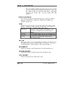
Page 66: ...rive specifications x Type The BIOS contains a table of pre defined drive types Each defined drive type has a specified number of cylinders number of heads write precompensation factor landing zone and number of sectors Drives whose specifications do not accommodate any predefine type are classified as type USER x Size Disk drive capacity approximate Note that this size is usually greater than the...

Page 67: ...ave to select the type in Setup Available Options are as follows EGA VGA Enhanced Graphics Adapter Video Graphics Array For EGA VGA SEGA SVGA or PGA monitor adapters CGA 40 Color Graphics Adapter power up in 40 column mode CGA 80 Color Graphics Adapter power up in 80 column mode MONO Monochrome adapter includes high resolution monochrome adapters HALT ON This category allows user to choose whether...

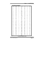
Page 68: ... 733 5 300 732 17 30 21 733 7 300 732 17 42 22 733 5 300 733 17 30 23 306 4 0000 336 17 10 24 977 5 65535 976 17 40 25 1024 9 65535 1023 17 76 26 1224 7 65535 1223 17 71 27 1224 11 65535 1223 17 111 28 1224 15 65535 1223 17 152 29 1024 8 65535 1023 17 68 30 1024 11 65535 1023 17 93 31 918 11 65535 1023 17 83 32 925 9 65535 926 17 69 33 1024 10 65535 1023 17 85 34 1024 12 65535 1023 17 102 35 1024 ...

Page 69: ...Mode MPS Version Control For OS OS Select for DRAM 64MB HDD S M A R T Capability Small Logo EPA Show Enabled Enabled Floppy HDD 0 CD ROM Enabled Disabled Disabled On Fast Disabled 6 250 Setup Enable 1 4 Non OS2 Disabled Disabled Menu Level Ź npom Move Enter Select PU PD Value F10 Save ESC Exit F1 General Help F5 Previous Values F6 Fail Safe Defaults F7 Optimized Defaults BIOS Features Setup Menu T...

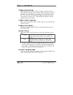
Page 70: ...OT DEVICE The BIOS attempt to load the operating system from the devices in the sequence selected in these items SWAP FLOOPY DRIVE This field is effective only in systems with two floppy drives Selecting Enabled assigns physical drive B to logical drive A and physical drive A to logical drive B BOOT UP FLOPPY SEEK You may enable disable this item to define whether the system will look for a floppy...

Page 71: ... the key is held down before it begins to repeat the keystroke SECURITY OPTION This category allows you to limit access to the system and Setup or just to Setup System The system will not boot and access to Setup will be denied if the correct password is not entered at the prompt Setup The system will boot but access to Setup will be denied if the correct password is not entered at the prompt To d...

Page 72: ...1024 LVDS Disabled Item Help Menu Level Ź npom Move Enter Select PU PD Value F10 Save ESC Exit F1 General Help F5 Previous Values F6 Fail Safe Defaults F7 Optimized Defaults Chipset Features Setup Screen This parameter allows you to configure the system based on the specific features of the installed chipset The chipset manages bus speed and access to system memory resources such as DRAM and the e...

Page 73: ...RECHARGE If an insufficient number of cycles is allowed for the RAS to accumulate its charge before DRAM refresh the refresh may be incomplete and the DRAM may fail to retain data Fast gives faster performance and Slow gives more stable performance This field applies only when synchronous DRAM is installed in the system SYSTEM BIOS CACHEABLE Selecting Enabled allows caching of the system BIOS ROM ...

Page 74: ...es Select Enabled to support compliance with PCI specification version 2 1 AGP APERTURE SIZE This field determines the effective size of the Graphic Aperture used for a particular GMCH configuration It can be updated by the GMCH specific BIOS configuration sequence before the PCI standard bus enumeration sequence takes place If it is not updated then a default value will select an aperture of maxi...

Page 75: ...x KB Power ON Password x Hot Key Power ON Onboard FDC Controller Onboard Serial Port 1 Onboard Serial Port 2 UART Mode Select x RxD TxD Active x IR Transmission Delay x UR2 Duplex Mode x Use IR Pins Onboard Parallel Port Parallel Port Mode x EPP Mode Select x ECP Mode Use DMA PWRON After PWR Fail Watch Dog Timer Select Onboard Serial Port 3 Onboard Serial Port 4 Enabled Auto Auto Auto Auto Enabled...

Page 76: ...sively increased performance In Auto mode the system automatically determines the best mode for each device IDE PRIMARY MASTER SLAVE UDMA IDE SECONDARY MASTER SLAVE UDMA Ultra DMA 33 implementation is possible only if your IDE hard drive supports it and the operating environment includes a DMA driver Windows 95 OSR2 or a third party IDE bus master driver If you hard drive and your system software ...

Page 77: ...his item allows you the select power on event KB POWER ON PASSWORD This item allows you to set the keyboard power on password HOT KEY POWER ON This item allows you to select the hot key of the keyboard power on The choice Ctrl F1 F12 ONBOARD FDC CONTROLLER Select Enabled if the system has a floppy disk controller FDC installed on the system board and you wish to use it If you install and in FDC or...

Page 78: ...This item allows you to determine access onboard parallel port controller with which I O address PARALLEL PORT MODE Select an operating mode for the onboard parallel printer port Select Normal Compatible or SPP unless you are certain your hardware and software both support one of the other available modes EPP MODE SELECT Select EPP port type 1 7 or 1 9 ECP MODE USE DMA Select a DMA channel for the...

Page 79: ... Port Enabled User Define 3 Disabled Instant Off Enabled Disabled 0 0 0 0 Disabled Disabled Disabled Disabled Disabled Item Help Menu Level Ź npom Move Enter Select PU PD Value F10 Save ESC Exit F1 General Help F5 Previous Values F6 Fail Safe Defaults F7 Optimized Defaults Power Management Setup Screen The Power Management Setup allows the user to configure the system to the most effectively save ...

Page 80: ...y 4 Sec and Instant Off WAKE UP BY PCI CARD An input signal from PME on the PCI card awakens the system from a soft off state RESUME BY ALARM When Enabled your can set the date and time at which the RTC real time clock alarm awakens the system from Suspend mode PM EVENTS PM events are I O events whose occurrence can prevent the system from entering a power saving mode or can awaken the system from...

Page 81: ...lues F6 Fail Safe Defaults F7 Optimized Defaults PNP PCI Configuration Setup Screen This section describes how to configure PCI bus system PCI also known as Personal Computer Interconnect is a system which allows I O devices to operate at speeds nearing the speed of the CPU itself uses when communica ting with its own special components This section covers technical items which is strongly recomme...

Page 82: ...ws 95 By choosing manual you are allowed to configure the IRQ Resources DMA Resources and Memory Resources The choices are Auto ESCD and Manual IRQ RESOURCES You may assign each system interrupt a type depending on the type of device using the interrupt DMA RESOURCES When resources are controlled manually assign each system DMA channel a type depending on the type of device using the DM channel PC...

Page 83: ... 02V 11 91V 12 36V 4 99V 3 36V 4 96V 75qC 167qF Item Help Menu Level Ź npom Move Enter Select PU PD Value F10 Save ESC Exit F1 General Help F5 Previous Values F6 Fail Safe Defaults F7 Optimized Defaults PC Health Status Setup Screen The setup menu allows you to select whether to choose between monitoring or ignoring the hardware monitoring function of your system CPU WARNING TEMERATURE This item w...

Page 84: ...ou the current SYSTEMFAN speed VCORE This item shows you the current system voltage 3 3V 5V 12V 12V 5V This item shows you the voltage of 3 3V 5V 12V 12V 5V SHUTDOWN TEMPERATURE This item allows you to set the CPU shutdown Temperature This function is only effective under Window 98 ACPI mode PC 5151 USER MANUAL Page 4 23 ...

Page 85: ... Help Menu Level Ź npom Move Enter Select PU PD Value F10 Save ESC Exit F1 General Help F5 Previous Values F6 Fail Safe Defaults F7 Optimized Defaults Frequency Voltage Control Setup Screen This setup menu allows you to specify your settings for frequency voltage control AUTO DETECT DIMM PCI CLK This item allows you to enable or disable auto detect DIMM PCI Clock SPREAD SPECTRUM This item allows y...

Page 86: ...power up the system Please be aware that if select the wrong panel type it may cause the abnormal display of the LCD 4 12 LOAD OPTIMIZED DEFAULTS When you press Enter on this category you get a confirmation dialog box with a message similar to the following Load Optimized Defaults Y N N Pressing Y loads the default values that are factory setting for optimal performance system operations Please be...

Page 87: ...assword typed now will clear any previously entered password from CMOS memory You will be asked to confirm the password Type the password again and press the Enter key You may also press Esc to abort the selection and not enter a password User should bear in mind that when a password is set you will be asked to enter the password everything you enter CMOS setup Menu TO DISABLE THE PASSWORD To disa...

Page 88: ...ipherals ŹFrequency Voltage Control Load Fail Safe Defaults Load Optimized Defaults Set Supervisor Password ŹPower Management ŹPnP PCI Configura ŹPC Health Status Save to CMOS and EXIT Y N Y word etup Saving Esc Quit F9 Menu in BIOS npom Select Item F10 Save Exit Setup Save Data to CMOS When you confirm that you wish to save the settings your system will be automatically restarted and the changes ...

Page 89: ...enix AwardBIOS CMOS Setup Utility ŹStandard CMOS Features ŹAdvanced BIOS Features ŹAdvanced Chipset Features ŹIntegrated Peripherals ŹFrequency Voltage Control Load Fail Safe Defaults Load Optimized Defaults Set Supervisor Password ŹPower Management ŹPnP PCI Configura Quit Without Saving Y N N word etup ŹPC Health Status Saving Esc Quit F9 Menu in BIOS npom Select Item F10 Save Exit Setup Abandon ...

Page 90: ...r Removing Back Cover z Exploded Diagram for Removing LCD Assembly z Exploded Diagram for Front Panel z Exploded Diagram for Removing CD ROM Assembly z Exploded Diagram for Removing HDD Assembly z Exploded Diagram for Removing Power z Exploded Diagram for Removing Output Panel z Exploded Diagram for Removing Motherboard z Exploded Diagram for Removing FDD CD ROM z Exploded Diagram for Removing Mas...

Page 91: ...Appendix A System Assembly EXPLODED DIAGRAM FOR REMOVING ARM HOLDER The Arm Holder does not support 3P3I Riser card module and PPC 7407 system Page A 2 PC 5151 USER MANUAL ...

Page 92: ...Appendix A System Assembly EXPLODED DIAGRAM FOR REMOVING HOOK HOLDER PC 5151 USER MANUAL Page A 3 ...

Page 93: ...Appendix A System Assembly EXPLODED DIAGRAM FOR REMOVING EXT CASE Page A 4 PC 5151 USER MANUAL ...

Page 94: ...Appendix A System Assembly EXPLODED DIAGRAM FOR REMOVING BACK COVER PC 5151 USER MANUAL Page A 5 ...

Page 95: ...Appendix A System Assembly EXPLODED DIAGRAM FOR REMOVING LCD ASSEMBLY Diagram 1 Page A 6 PC 5151 USER MANUAL ...

Page 96: ...Appendix A System Assembly Diagram 2 PC 5151 USER MANUAL Page A 7 ...

Page 97: ...Appendix A System Assembly EXPLODED DIAGRAM FOR FRONT PANEL Diagram 1 Page A 8 PC 5151 USER MANUAL ...

Page 98: ...Appendix A System Assembly Diagram 2 PC 5151 USER MANUAL Page A 9 ...

Page 99: ...Appendix A System Assembly EXPLODED DIAGRAM FOR REMOVING CD ROM ASSEMBLY Page A 10 PC 5151 USER MANUAL ...

Page 100: ...Appendix A System Assembly EXPLODED DIAGRAM FOR REMOVING HDD ASSEMBLY PC 5151 USER MANUAL Page A 11 ...

Page 101: ...Appendix A System Assembly EXPLODED DIAGRAM FOR REMOVING MOTHERBOARD AND POWER Page A 12 PC 5151 USER MANUAL ...

Page 102: ...Appendix A System Assembly EXPLODED DIAGRAM FOR REMOVING OUTPUT PANEL PC 5151 USER MANUAL Page A 13 ...

Page 103: ...Appendix A System Assembly EXPLODED DIAGRAM FOR REMOVING FDD CD ROM Diagram 1 Remove FDD Page A 14 PC 5151 USER MANUAL ...

Page 104: ...Appendix A System Assembly Diagram 2 Remove CD ROM PC 5151 USER MANUAL Page A 15 ...

Page 105: ...Appendix A System Assembly EXPLODED DIAGRAM FOR REMOVING MASK Page A 16 PC 5151 USER MANUAL ...

Page 106: ...Appendix A System Assembly EXPLODED DIAGRAM FOR WALL MOUNTING Diagram 1 PC 5151 USER MANUAL Page A 17 ...

Page 107: ...Appendix A System Assembly Diagram 2 PS 8170A PS 8150A Page A 18 PC 5151 USER MANUAL ...

Page 108: ...Appendix A System Assembly Diagram 3 Diagram 4 PC 5151 USER MANUAL Page A 19 ...

Page 109: ...TECHNICAL SUMMARY APPENDIX B This section introduce you the maps concisely Sections include z Block Diagram z Interrupt Map z RTC Standard RAM Bank z Timer DMA Channels Map z I O Memory Map Page B 1 ...

Page 110: ...Appendix B Technical Summary BLOCK DIAGRAM Page B 2 PC 5151 USER MANUAL ...

Page 111: ...ard output buffer full 2 Cascade for IRQ 8 15 3 Serial port 2 4 Serial port 1 5 Available 6 Floppy Disk adapter 7 Parallel port 1 8 RTC clock 9 ACPI Compliant System 10 Serial port 3 11 Serial port 4 12 PS 2 Mouse 13 Math coprocessor 14 Hard Disk adapter 15 Hard Disk adapter PC 5151 USER MANUAL Page B 3 ...

Page 112: ...onds 01h Second alarm 02h Minutes 03h Minutes alarm 04h Hours 05h Hours alarm 06h Day of week 07h Day of month 08h Month 09h Year 0Ah Status register A 0Bh Status register B 0Ch Status register C 0Dh Status register D 0Eh 7Fh 114 Bytes of User RAM Page B 4 PC 5151 USER MANUAL ...

Page 113: ... Timer Channel Assignment 0 System timer interrupt 1 DRAM Refresh request 2 Speaker tone generator DMA Channel Map DMA Channel Assignment 0 Available 1 Available 2 Floppy Disk adapter 3 Available 4 Cascade 5 Available 6 Available 7 Available PC 5151 USER MANUAL Page B 5 ...

Page 114: ...ller Interrupt 3Ch 3Dh Interrupt Controller Interrupt Controller Interrupt 40h 42h Timer Counter Timer Counter PIT 8254 43h Reserved Timer Counter PIT 4E 4F LPC SIO LPC SIO Forwarder to LPC 50h 52h Timer Counter Timer Counter PIT 53h Reserved Timer Counter PIT 60h Microcontroller Microcontroller Forwarder to LPC 61h NMI Controller NMI Controller Processor I F 62h Microcontroller Microcontroller Fo...

Page 115: ...ower Management Power Management B4h B5h Interrupt Controller Interrupt Controller Interrupt B8h B9h Interrupt Controller Interrupt Controller Interrupt BCh BDh Interrupt Controller Interrupt Controller Interrupt C0h D1h DMA Controller DMA Controller DMA D2h DDh Reserved DMA Controller DMA DEh DFh DMA Controller DMA Controller DMA F0h See Note 3 FERR IGNNE Interrupt Controller Processor interface ...

Page 116: ...00h FF3F FFFFh FF60 0000h FF6F FFFFh FF20 0000h FF2F FFFFh FF50 0000h FF5F FFFFh FF10 0000h FF1F FFFFh FF40 0000h FF4F FFFFh FF00 0000h FF0F FFFFh FWH Bit 0 in FWH Decode Enable Register FWH Bit 1 in FWH Decode Enable Register FWH Bit 2 in FWH Decode Enable Register is set FWH Bit 3 in FWH Decode Enable Register is set FWH Bit 4 in FWH Decode Enable Register is set FWH Bit 5 in FWH Decode Enable R...

Reviews: