


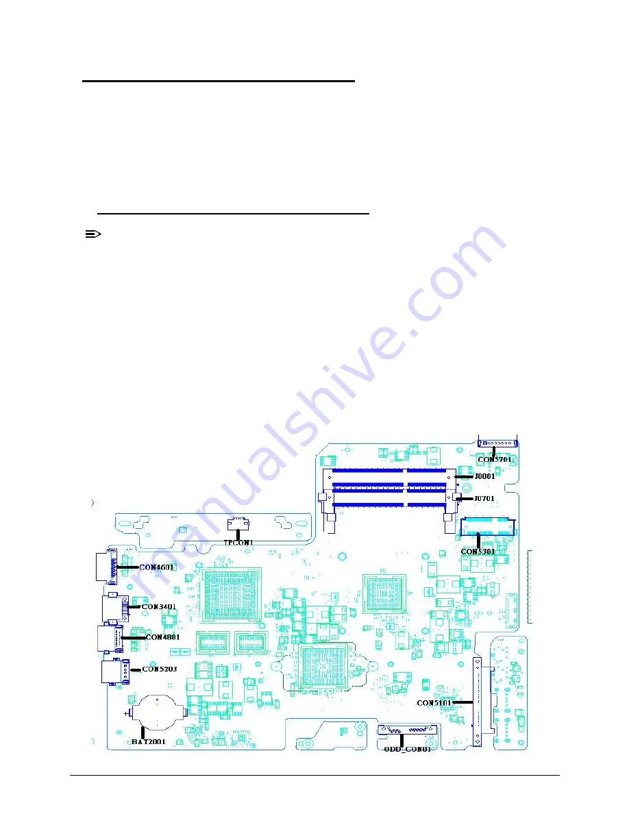
Jumper and Connector Locations
5-7
Clearing Password Check and BIOS Recovery
0
This section provides procedures for:
Clearing Passwords
BIOS Recovery.
This Machine has one Hardware Open Gap on the main board for clearing password check
and one Hotkey for enabling BIOS Recovery.
Clearing Password Check
0
NOTE:
NOTE
:
The following procedure is only for clearing BIOS Password (Supervisor Password and
User Password).
Steps for Clearing BIOS Password Check
0
If users set BIOS Passwords (Supervisor Password and/or User Password) for a security
reason, BIOS will ask the password during systems POST or when system enters the BIOS
Setup menu. If it is necessary to bypass the password check, short the HW Gap to clear the
password by performing the following steps:
1.
Remove power from the system.
2.
Remove HDD, AC and Battery.
3.
Disconnect the RTC Battery (Figure 5-3 <BAT2001>).
Summary of Contents for Aspire 7250
Page 36: ...1 40 Hardware Specifications and Configurations ...
Page 45: ...System Utilities 2 11 Figure 2 9 Setup Warning ...
Page 64: ...2 30 System Utilities ...
Page 71: ...3 11 Figure 3 7 HDD Module Figure 3 8 HDD Module 3 Remove HDD follow the arrowhead ...
Page 72: ...3 12 Figure 3 9 HDD Module Figure 3 10 HDD Module ...
Page 74: ...3 14 Figure 3 13 WLAN Module ...
Page 77: ...3 17 Figure 3 19 Memory Module Figure 3 20 Memory Module Figure 3 21 Memory Module ...
Page 85: ...3 25 Figure 3 35 TOP Case Figure 3 36 TOP Case ...
Page 88: ...3 28 Figure 3 42 I O BD Figure 3 43 I O BD ...
Page 90: ...3 30 Figure 3 46 Mother board Figure 3 47 Mother board 3 Take out the RTC battery ...
Page 91: ...3 31 Figure 3 48 RTC BATTERY Figure 3 49 RTC BATTERY ...
Page 93: ...3 33 Figure 3 51 Thermal Figure 3 52 Thermal ...
Page 101: ...3 41 Figure 3 68 LCD Panel Figure 3 69 LCD Panel 3 Put camera and MIC in the right place ...
Page 102: ...3 42 Figure 3 70 LCD Panel Figure 3 71 LCD Panel ...
Page 105: ...3 45 Figure 3 76 Hinge ...
Page 108: ...3 48 Figure 3 81 Main board Figure 3 82 Main board ...
Page 110: ...3 50 Figure 3 85 ODD BD Figure 3 86 ODD BD 2 Connect IO BD and ODD B D FFC CONN ...
Page 111: ...3 51 Figure 3 87 IO BD Figure 3 88 ODD BD ...
Page 114: ...3 54 Figure 3 93 Top case Figure 3 94 Top case ...
Page 116: ...3 56 Figure 3 97 Top case Figure 3 98 Top case Figure 3 99 Top case ...
Page 121: ...3 61 Figure 3 108 ...
Page 125: ...3 65 Figure 3 115 Battery ...
Page 126: ...3 66 ...
Page 152: ...4 28 Troubleshooting ...
Page 155: ...Jumper and Connector Locations 5 5 Figure 5 2 Mainboard Bottom ...
Page 160: ...5 10 Jumper and Connector Locations ...
Page 186: ...6 28 FRU Field Replaceable Unit List ...
Page 215: ...Test Compatible Components 8 11 ...
Page 216: ...8 12 Test Compatible Components ...
Page 217: ...Test Compatible Components 8 13 ...
Page 218: ...8 14 Test Compatible Components ...
Page 219: ...Test Compatible Components 8 15 ...
Page 220: ...8 16 Test Compatible Components ...
Page 221: ...Test Compatible Components 8 17 ...
Page 222: ...8 18 Test Compatible Components ...