background image

Warranty


Prior to shipment, ACCES equipment is thoroughly inspected and tested to applicable specifications. However, 
should equipment failure occur, ACCES assures its customers that prompt service and support will be available. 
All equipment originally manufactured by ACCES which is found to be defective will be repaired or replaced 
subject to the following considerations. 
 

Terms and Conditions


If a unit is suspected of failure, contact ACCES' Customer Service department. Be prepared to give the unit 
model number, serial number, and a description of the failure symptom(s). We may suggest some simple tests 
to confirm the failure. We will assign a Return Material Authorization (RMA) number which must appear on the 
outer label of the return package. All units/components should be properly packed for handling and returned 
with freight prepaid to the ACCES designated Service Center, and will be returned to the customer's/user's site 
freight prepaid and invoiced. 
 

Coverage


First Three Years: Returned unit/part will be repaired and/or replaced at ACCES option with no charge for labor 
or parts not excluded by warranty. Warranty commences with equipment shipment. 
 
Following Years: Throughout your equipment's lifetime, ACCES stands ready to provide on-site or in-plant 
service at reasonable rates similar to those of other manufacturers in the industry. 
 

Equipment Not Manufactured by ACCES


Equipment provided but not manufactured by ACCES is warranted and will be repaired according to the terms 
and conditions of the respective equipment manufacturer's warranty. 
 

General


Under this Warranty, liability of ACCES is limited to replacing, repairing or issuing credit (at ACCES discretion) 
for any products which are proved to be defective during the warranty period. In no case is ACCES liable for 
consequential or special damage arriving from use or misuse of our product. The customer is responsible for all 
charges caused by modifications or additions to ACCES equipment not approved in writing by ACCES or, if in 
ACCES opinion the equipment has been subjected to abnormal use. "Abnormal use" for purposes of this 
warranty is defined as any use to which the equipment is exposed other than that use specified or intended as 
evidenced by purchase or sales representation. Other than the above, no other warranty, expressed or implied, 
shall apply to any and all such equipment furnished or sold by ACCES. 


Manual 104-DIO-48E, 24E 

3

Summary of Contents for 104-DIO-24E

Page 1: ...service in house repair center WE BUY USED EQUIPMENT Sell your excess underutilized and idle used equipment We also offer credit for buy backs and trade ins www artisantg com WeBuyEquipment REMOTE IN...

Page 2: ...10623 Roselle Street San Diego CA 92121 y 858 550 9559 y Fax 858 550 7322 contactus accesio com y www accesio com MODEL 104 DIO 48E and 104 DIO 24E USER MANUAL FILE M104 DIO 48E A1n...

Page 3: ...s IBM PC PC XT and PC AT are registered trademarks of the International Business Machines Corporation Printed in USA Copyright 2001 2005 by ACCES I O Products Inc 10623 Roselle Street San Diego CA 921...

Page 4: ...warranty Warranty commences with equipment shipment Following Years Throughout your equipment s lifetime ACCES stands ready to provide on site or in plant service at reasonable rates similar to those...

Page 5: ...ng Your Application Software 15 Table 5 1 Address Selection Table 15 Digital I O 16 Table 5 2 Control Register Bit Assignment 16 Programming Example Basic 18 Enabling Disabling I O Buffers 18 Counter...

Page 6: ...Peripheral Interface PPI chips of type 82C55 to provide a computer interface to 48 I O lines There are three 8 bit ports A B and C per PPI Each 8 bit port can be configured by software to function as...

Page 7: ...board optionally has an 82C54 Counter Timer chip This can be used for frequency measurement frequency output pulse width modulation pulse width measurement event count etc SPECIAL NOTE FOR PROGRAMMERS...

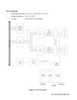
Page 8: ...SELECT INTERRUPT ENABLE PPI GROUP 1 PPI GROUP 0 DI O INTERRUPT COMPUTER I O BUS I O B U F F E R S C O N N E C T O R C O N N E C T O R PORT A PORT B PORT C HI PORT C LO PORT A PORT B PORT C HI PORT C L...

Page 9: ...n The following instructions assume the CD ROM drive is drive D Please substitute the appropriate drive letter for your system as necessary DOS 1 Place the CD into your CD ROM drive 2 Type B to change...

Page 10: ...ess according to your application requirements as mentioned above 2 Remove power from the PC 104 stack 3 Assemble standoff hardware for stacking and securing the boards 4 Carefully plug the board onto...

Page 11: ...upts are enabled by writing any value to base address Bh and disabled by reading from that address Once an interrupt has occured it must be cleared by writing any value to base address Fh for the next...

Page 12: ...A4 A5 A6 A7 A8 IRQ 12 IRQ 4 IRQ 5 IRQ 7 IRQ 10 IRQ 11 P1 P4 P3 IRQ 3 A9 Pin 1 Pin 1 Pin 1 IEN1 IEN0 INP1 INP0 TST BEN Figure 3 1 Option Selection Map Manual 104 DIO 48E 24E 11...

Page 13: ...A 2C0 2CF EGA 2D0 2DF EGA 2E0 2E7 GPIB AT 2E8 2EF Serial Port 2F8 2FF Serial Port 300 30F Prototype Board 310 31F Prototype Board 320 32F Hard Disk XT 370 377 Floppy Controller 2 378 37F Parallel Prin...

Page 14: ...300h 30Fh On 2F0h 2FFh On On 2E0h 2EFh On On 2D0h 2DFh On On On 2C0h 2CFh On On 2B0h 2BFh On On On 2A0h 2AFh On On On 290h 29Fh On On On On 280h 28Fh On On 270h 27Fh On On On 260h 26Fh On On On 250h 2...

Page 15: ...evious page before selecting the board address If the addresses of two circuits overlap you will experience unpredictable computer behavior Note that address ranges 100h 10Fh through 1F0h 1FFh can be...

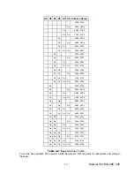
Page 16: ...ister Operation Counter Timer Disabled Counter Timer Enabled Base Address PA Group 0 Counter Timer 0 Read Write Base Address 1 PB Group 0 Counter Timer 1 Read Write Base Address 2 PC Group 0 Counter T...

Page 17: ...put 0 Output D2 Mode Select 1 Mode 1 0 Mode 0 D3 Port C Hi C4 C7 1 Input 0 Output D4 Port A 1 Input 0 Output D5 D6 Mode Select 00 Mode 0 01 Mode 1 1X Mode 2 D7 Mode Set Flag 1 Active Table 5 2 Control...

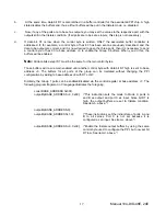
Page 18: ...t be the same for the two control bytes Those buffers will now remain enabled until another control byte with data bit D7 high is sent to base address 3 The buffers for all ports of the group can be t...

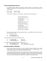
Page 19: ...0 X INP BASEADDR Read Port A 40 Y INP BASEADDR 2 16 Read Port C Hi To set outputs high 1 at Port B and the lower nybble of Port C 50 OUT BASEADDR 1 HFF Turn on all Port B bits 60 OUT BASEADDR 2 HF Tur...

Page 20: ...the mode you must first set the new mode and then enable the buffers Enabling the buffers can be done at either Base Address 3 or 7 or Base Address 8 or 9 Counter Timer The board uses an 8254 counter...

Page 21: ...o indicate that it asserted the interrupt but is otherwise capable of sharing the IRQ In this case it may share the interrupt level with other boards if a it is the only board on that IRQ level that d...

Page 22: ...Count After the counter is loaded the output is set low and will remain low until the counter decrements to zero The output then goes high and remains high until a new count is loaded into the counte...

Page 23: ...gger Programming the 8254 The counters are programmed by writing a control byte into the counter control register The control byte specifies the counter to be programmed the counter mode the type of r...

Page 24: ...ter on the fly without disturbing the counting process You can only rely on directly read counter data if the counting process is suspended while reading by bringing the gate low For each counter you...

Page 25: ...s in BCD mode If both STA and CNT bits in the readback command byte are set low and the RW1 and RW0 bits have both been previously set high in the counter control register thus selecting two byte read...

Page 26: ...is limited by the input speed of the 8254 counter and slow signals are preferred Further only 65 535 events are possible without a RESET The function returns the number of events based on priority or...

Page 27: ...ut PPI 0 write any value to Base Address Dh To map out the counter timer and map in PPI 0 read from Base Address Dh This mapping does not reset either chip in any way so you can for example map in the...

Page 28: ...ery second line is grounded to minimize crosstalk between signals Table 7 1 Digital I O P3 and P4 Connector Pin Assignments Assignment Pin Assignment Pin PC7 1 2 PC6 3 4 PC5 5 6 Port C Hi PC4 7 8 PC3...

Page 29: ...nector Pin Assignments Assignment Pin Ground 1 Ground 2 1MHz Clock output 3 Ground 4 Clock 0 a k a CLOCK IN events input 5 Ground 6 Gate 1 a k a GATE IN input 7 Ground 8 Output 2 a k a CLOCK OUT 9 Gro...

Page 30: ...ve us some feedback please email us at manuals accesio com Please detail any errors you find and include your mailing address so that we can send you any manual updates 10623 Roselle Street San Diego...

Page 31: ...service in house repair center WE BUY USED EQUIPMENT Sell your excess underutilized and idle used equipment We also offer credit for buy backs and trade ins www artisantg com WeBuyEquipment REMOTE IN...

Reviews: