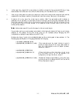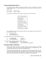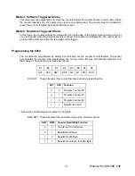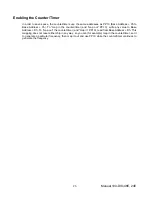
Two computer I/O bus addresses are available that permit you to enable or disable the I/O buffers at
will, without programming the PPI mode. Buffers for Goup 0 bits are enabled/disabled at Base Address
+8 and buffers for Group 1 bits are enabled/disabled at Base A9. To enable the buffers and to
set outputs to the desired state, you can write to the Control Register with bit D7 low. If you wish to
subsequently disable the buffers, you can write to the Control Register with bit D7 high. In this way you
can enable/disable the output buffers without programming the PPI mode.
Note
When writing a command byte to the board while the TST jumper is installed, the PPI output buffers are
disabled. Thus, when you desire to change the mode, you must first set the new mode and then enable the
buffers. Enabling the buffers can be done at either Base A3 (or +7) or Base A8 (or +9).
Counter/Timer
The board uses an 8254 counter/timer chip to provide three counter/timers.
In order to save space, the counter/timers use the same addresses as PPI 0 (Base A 0h to
Base A 3h). To “map in the counter/timer (and “map out” PPI 0), write any value to Base
A Dh. To “map out” the counter/timer (and “map in” PPI 0), read from Base A Dh. This
mapping does not reset either chip in any way, so you can (for example) map in the counter/timer, set it
to generate a particular frequency, then map it out and use PPI 0 while the counter/timer continues to
generate the frequency.
The counter/timer has a variety of uses: event counting, frequency measurement, frequency
generation. See the 8254 Counter/Timer chapter for details on how to use it.
Manual 104-DIO-48E, 24E
19

