UM031 FMC168/4/2
r1.7
UM031
page 27 of 28
Appendix C
CPLD Register map
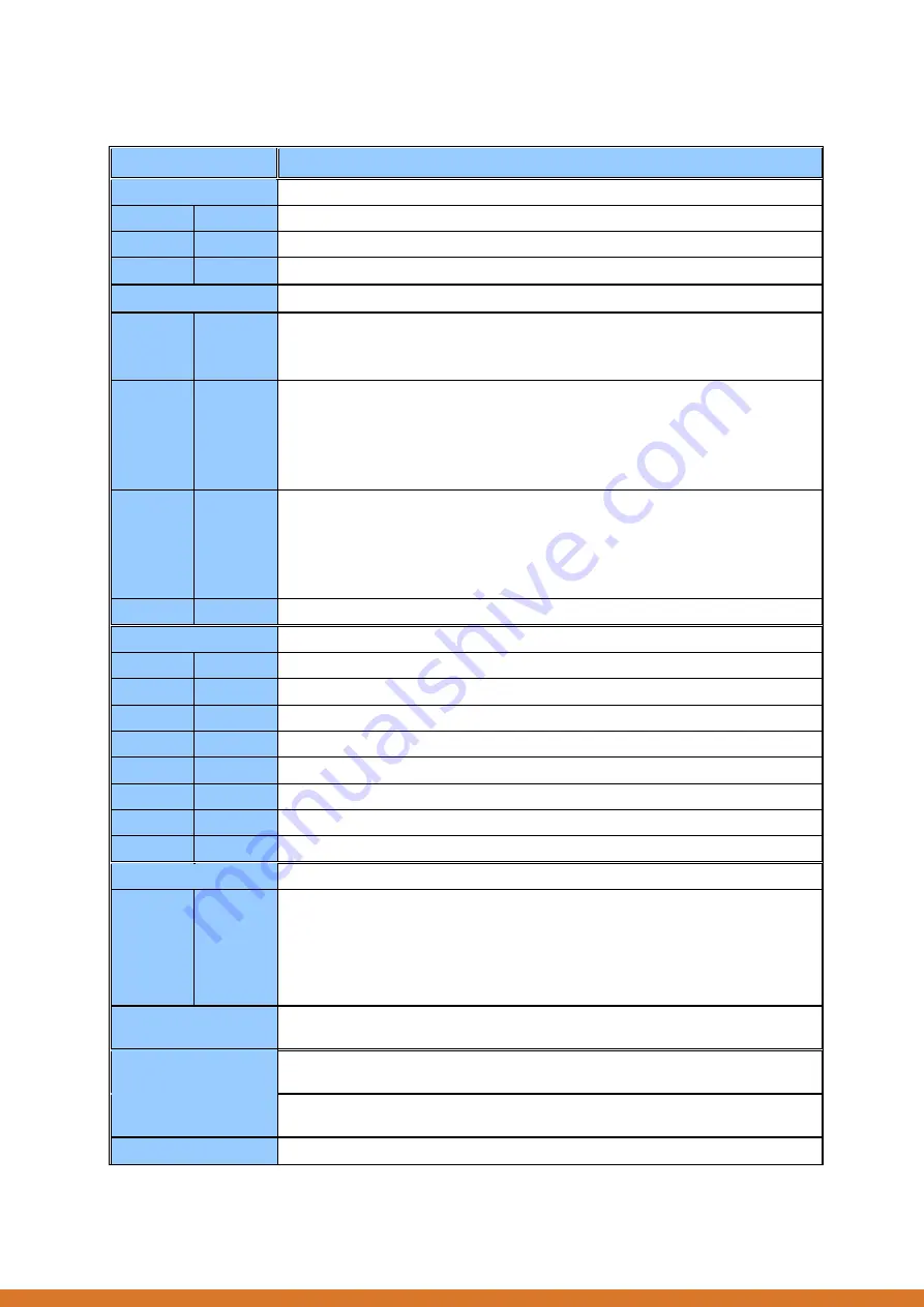
Register
Description
0x00
Command register (Write only, defaults to 0x00)
Bit 0
Clock tree (AD9517) reset, This bit is self-clearing
Bit 1
ADC (ADS42LB69) reset
Bit 2..7
Reserved
0x01
Control register (Read/Write, defaults to 0x1D)
Bit 0
VCO Enable (not available on r1.0 boards)
‘0’ Onboard VCO disabled
‘1’ Onboard VCO enabled
Bit 3..1
Clock Source Select:
“000” for external clock
“011” for internal clock with external reference
“110” for internal clock with internal reference
Other combinations should not be used
Bit 5..4
Sync Source Select:
“00” for external trigger
“01” for CPLD (Forced to inactive state in CPLD)
“10” for Clock Tree
“00” for FPGA (FMC CLK2_BIDIR_P/N connection)
Bit 7..6
Reserved for future use, write “00”.
0x02
Status register (Read only)
Bit 0
Always ‘0’
Bit 1
Always ‘0’
Bit 2
Level of STATUS output from AD9517
Bit 3
Level of REFMON output from AD9517
Bit 4
Level of LD output from AD9517
Bit 5
Always ‘0’
Bit 6
Always ‘0’
Bit 7
Level of ALERT output from AD7291
0x03
Version register (Read only)
Bit 7..0
“0x2A”
initial release with basic functions. SPI readback from ADC devices is not
available. Command register not available. Two LSB of I2C address fixed to “00”.
“0x2B”
added support for SPI readback from ADC devices. Added reset controls
through command register. Two LSB of I2C address set by GA[1..0].
“0x2C”
enabled control for VCO (Register 0x01, Bit 0). This CPLD version should
not be used on r1.0 boards.
0x04
Byte 0 (write only),
writing to this register sets bit 7..0 in the internal 24-bit control
word.
0x05
Byte 1 (write only),
writing to this register sets bit 15..8 in the internal 24-bit control
word.
0x06
Byte 2 (write only),
writing to this register sets bit 23..16 in the internal 24-bit control
word.
0x07
Device Select (write only),
writing the register values below will initiate a SPI cycle