background image

52

    SBC-554V/555 User's Manual

Save & exit setup

If you select this option and press <Enter>, the values entered in
the setup utilities will be recorded in the chipset's CMOS memory.
The microprocessor will check this every time you turn your
system on and compare this to what it finds as it checks the
system. This record is required for the system to operate.

Exit without saving

Selecting this option and pressing <Enter> lets you exit the Setup
program without recording any new values or changing old ones.

Summary of Contents for SBC-555

Page 1: ...SBC 554V Half size 586 CPU Card with PISA Bus SBC 555 Half size 586 CPU Card with ISA Bus ...

Page 2: ...VICE PURSUANT TO PART 15 OF THE FCC RULES THESE LIMITS ARE DESIGNED TO PROVIDE REASON ABLE PROTECTION AGAINTST HARMFUL INTERFER ENCE WHEN THE EQUIPMENT IS OPERATED IN A COMMERCIAL ENVIRONMENT THIS EQUIPMENT GENERATES USES AND CAN RADIATE RADIO FREQENCY ENERGY AND IF NOT INSTATLLED AND USED IN ACCORDANCE WITH THE INSTRUCTION MANUAL MAY CAUSE HARMFUL INTERFERENCE TO RADIO COMMUNICATIONS OPERATION OF...

Page 3: ...nc AutoCAD and AutoShade are trademarks of Autodesk Inc CHIPS Logotype is a registered trademark Chips 65554 is a trademark of Chip and Technologies Inc Cyrix is a trademark of Cyrix Corporation IBM PC AT PS 2 and VGA are trademarks of International Business Machines Corporation Intel and Pentium are trademarks of Intel Corporation Lotus 1 2 3 an Symphony are trademarks of Lotus Development Corp M...

Page 4: ...i DIN dual outlet adapter for keyboard and PS 2 mouse 1 Hard disk drive IDE interface cable 40 pin 1 Floppy disk drive interface cable 34 pin 1 Parallel port adapter 26 pin and COM2 adapter 9 pin kit 4 Utility disks with CHIPS 65554 utility programs and drivers If any of these items are missing or damaged contact your distributor or sales representative immediately ...

Page 5: ...oltage Setting JP2 15 Vcore voltage setting JP4 16 CPU I O Voltage setting JP3 17 PCI Bus Clock Sync Async Mode settings JP5 17 CPU External Clock Selection JP6 17 CPU Jumper Setting Example 18 LCD Panel s Voltage setting JP7 19 Clear CMOS Data JP8 19 SSD Address settings JP9 19 RS 232 422 485 selections JP10 20 Hardware Reset JP11 20 Installing SIMMs 21 Removing SIMMS 21 IDE hard drive connector ...

Page 6: ...IOS Setup 29 System test and initialization 30 System configuration verification 30 AWARD BIOS setup 31 Entering setup 31 Standard CMOS setup 32 BIOS features setup 33 Virus Warning 33 CHIPSET features setup 36 Power management setup 38 PM Timers 40 PM Events 40 PnP PCI Configuration setup 42 Load BIOS DEFAULTs LOAD SETUP DEFAULTS 44 Integrated Peripherals 45 Internal PCI IDE 45 Supervisor User Pa...

Page 7: ...ivers 54 Hardware configuration 54 Necessary prerequisites 55 Before you begin 55 WindowsÔ 95 Ô 95 Ô 95 Ô 95 Ô 95 56 WindowsÔ 3 1 Ô 3 1 Ô 3 1 Ô 3 1 Ô 3 1 57 OS 2 58 WindowsÔ NT3 51 Ô NT3 51 Ô NT3 51 Ô NT3 51 Ô NT3 51 60 Windows NT4 0 61 Appendix A Programming the Watchdog Timer 63 ...

Page 8: ......

Page 9: ...Chapter 1 General Information 1 1 General Information This chapter provides background information for the SBC 554V 555 Sections include Card specifications Board layout C H A P T E R ...

Page 10: ...re of the SBC 554V 555 is the inclusion of a high speed local bus IDE controller This controller supports through ATA PIO mode 3 and mode 4 hard disks and Ultra DMA 33 enabling data transfer rates up to 33MB second Up to two IDE devices can be connected including large hard disks CD ROM drives tape backup drives or other IDE devices On board features include two high speed RS 232 serial ports with...

Page 11: ...2nd level cache VGA Controller C T 65554 with display memory 2MB on board Display type Support CRT and flat panel TFT DSTN MONO and EL display Can display both CRT and flat panel simultaneously Support resolution up to 1024x768 64K color FPD Link Flat Panel Display Link Optional function to support LVDS Low Voltage Differential Signaling for high speed and low power data transfer Disk On Chip One ...

Page 12: ...ppy disk drives 5 25 360KB and 1 2MB and or 3 5 720KB 1 44MB and 2 88MB Multi mode parallel port Configured to LPT1 LPT2 LPT3 ro disabled Supports SPP ECP and EPP Serial ports One RS 232 and one RS 232 422 485 serial ports Ports can be configured as COM1 COM2 COM3 COM4 or disabled individual ly Two 16C550 serial UARTs IR connector reserved for future use Keyboard mouse connector 6 pin mini DIN con...

Page 13: ...ion Support up to 1024x768 64K colors SSD interface One 32 pin DIP socket supports M system Disk On Chip 2000 series memory capacity from 1MB to 24MB Mechanical and environmental Power supply voltage 5V 4 75V to 5 25V 12V 11 4V to 12 6V Power Requirement Bare Board 5V 1 5A Pentium MMX 200 onboard 5V 6A K6 233 onboard 5V 10A Operating temperature 32 to 140 F 0 to 60 C Board size 7 3 L x 4 8 W 185 m...

Page 14: ...6 SBC 554V 555 User s Manual Board layout UMC UM8669F 14 318 DiskOnChip B A T S S T N H 2 9 E E 0 1 0 150 3CF 952827 E 5 5 8 2 S I S B 6 5 5 5 4 CHIPS ...

Page 15: ...Chapter 1 General Information 7 Card dimensions 185 00 178 00 122 00 98 50 19 50 D4x4 ...

Page 16: ...8 SBC 554V 555 User s Manual ...

Page 17: ...ter explains set up procedures for the SBC 554V 555 hardware including instructions on setting jumpers and connecting peripherals switches and indicators Be sure to read all safety precautions before you begin the installa tion procedure C H A P T E R ...

Page 18: ... clock Ratio JP2 DRAM Voltage setting JP3 VIO Voltage setting JP4 Vcore Voltage setting JP5 PCI clock setting JP6 CPU external clock selection JP7 LCD Panel s Voltage setting JP8 Clear CMOS Data JP9 SSD address setting JP10 RS232 422 485 selection JP11 Hardware Reset CN1 HDD connector CN2 FDD connector CN3 LCD connector CN4 USB connector CN5 Parallel connector CN6 COM2 connector CN7 COM1 connector...

Page 19: ... 1 8 DiskOnChip B A T S S T N H 2 9 E E 0 1 0 1 5 0 3 C F 9 5 2 8 2 7 E 5 5 8 2 S I S B65554 C H I P S COM2 CON PRINTER CON USB CON JP7 LCD CON FDD CON HDD CON CN13 HDD LED JP1 JP2 KB MOUSE CON CN11 INV JP9 JP8 JP6 JP5 JP3 JP4 CN12 IR 4 PIN POWER CON JP10 VGA CON COM1 CON JP11 ...

Page 20: ...a jumper you connect the pins with the clip To open a jumper you remove the clip Sometimes a jumper will have three pins labeled 1 2 and 3 In this case you would connect either pins 1 and 2 or 2 and 3 The jumper settings are schematically depicted in this manual as follows A pair of needle nose pliers may be helpful when working with jumpers If you have any doubt about the best hardware configurat...

Page 21: ... shielded bag when they are not in the chassis Installing the CPU The SBC 554V CPU card supports most Pentium and its compati ble CPUs The system s performance depends on the CPU you choose You can install or upgrade the CPU in the board s PGA socket by following the procedures outlined below If your system has an existing CPU you need to remove it before installing the new CPU Removing a CPU 1 Di...

Page 22: ... other components 2 Carefully align the CPU so that it is parallel to the socket Make sure that the notch on the corner of the CPU matches the notch on the inside of the socket 3 Gently push the CPU into the socket There will probably be a small gap between the CPU and the socket even when it is fully seated DO NOT USE EXCESSIVE FORCE When you install a new CPU you may have to adjust other setting...

Page 23: ... Default P54C x1 5 P54C x2 0 P54C x3 0 P54C x2 5 P55C x3 5 P55C x2 0 P55C x3 0 P55C x2 5 DRAM Voltage Setting JP2 SBC 554V 555 supports 5V DRAM and 3 3V DRAM JP 2 must be set to match the DRAM type 5V Default 3 3V AMD K6 x3 5 AMD K6 x2 0 AMD K6 x3 0 AMD K6 x2 5 AMD K6 x5 5 AMD K6 x4 0 AMD K6 x5 0 AMD K6 x4 5 6 5 4 3 2 1 6 5 4 3 2 1 6 5 4 3 2 1 6 5 4 3 2 6 5 4 3 2 1 6 5 4 3 2 1 6 5 4 3 2 1 6 5 4 3 ...

Page 24: ...tage settings JP 4 2 0V 2 1V 2 2V 2 3V 2 4V 2 5V 2 6V 2 7V 2 8V Default 2 9V 3 0V 3 1V 3 2V 3 3V 3 4 V 2 4 6 8 1 3 5 7 2 4 6 8 2 4 6 8 1 3 5 7 2 4 6 8 1 3 5 7 2 4 6 8 1 3 5 7 2 4 6 8 1 3 5 7 2 4 6 8 1 3 5 7 2 4 6 8 1 3 5 7 2 4 6 8 1 3 5 7 2 4 6 8 1 3 5 7 2 4 6 8 1 3 5 7 2 4 6 8 1 3 5 7 1 3 5 7 2 4 6 8 1 3 5 7 2 4 6 8 1 3 5 7 2 4 6 8 1 3 5 7 ...

Page 25: ... Async Mode settings JP5 JP 5 allows users to select Sync or Async PCI clock The Sync PCI clock depends on half of the CPU external clock in contrast the Async PCI Clock is fixed on 33MHz 33MHz 25MHz 30MHz 33MHz Async Mode setting Sync Mode setting Equal to 1 2 x CPU Ext CLK Default CPU External Clock Selection JP6 JP 6 allows users to select CPU External clock 50 MHz 60MHz 66MHz Default 1 2 3 1 2...

Page 26: ... 2 8V AMD K6 pr2 233 233MHz 66MHz 3 5 3 2V AMD K6 pr2 200 200MHz 66MHz 3 2 9V AMD K6 pr2 166 166MHz 66MHz 2 5 2 9V Cyrix 6 x 86 133MHz 66MHz 2 pr 166 3 4V 2 4 6 1 3 5 5 3 1 6 4 2 5 3 1 6 4 2 5 3 1 6 4 2 5 3 1 6 4 2 5 3 1 6 4 2 5 3 1 6 4 2 5 3 1 6 4 2 5 3 1 6 4 2 2 4 6 1 3 5 2 4 6 1 3 5 2 4 6 1 3 5 2 4 6 1 3 5 2 4 6 1 3 5 2 4 6 1 3 5 2 4 6 1 3 5 2 4 6 8 1 3 5 7 2 4 6 8 1 3 5 7 2 4 6 8 1 3 5 7 2 4 6...

Page 27: ...of LCD panel 5 V Default 3 3V Clear CMOS Data JP8 JP 8 allows users to clear CMOS data Normal Default Clear CMOS SSD Address settings JP9 You can select SDD address by setting JP9 Address CC000 D0000 D4000 Address D8000 Default DC000 2 4 6 1 3 5 2 4 6 1 3 5 2 4 6 1 3 5 2 4 6 1 3 5 1 2 3 1 2 3 1 2 3 1 2 3 2 4 6 1 3 5 ...

Page 28: ...er s Manual RS 232 422 485 selections JP10 You can configure COM2 as RS232 RS422 or RS485 by setting JP10 RS 232 Default RS 422 RS 485 Hardware Reset JP11 Normal Default Reset 6 4 2 5 3 1 6 4 2 5 3 1 6 4 2 5 3 1 2 1 2 1 ...

Page 29: ...on top of the vertical posts should corre spond to the circular holes on the ends of the module 3 Repeat steps 1 and 2 for each module you install Removing SIMMs If you need to remove a SIMM follow the procedures below 1 Supporting the SIMM with a finger use a pen or a similarly shaped object and press one retaining clip straight down 2 Repeat for the other side When released the retaining clips w...

Page 30: ...pin connector Wire number 1 on the cable is red or blue and the other wires are gray 1 Connect one end of the cable to CN1 Make sure that the red or blue wire corresponds to pin 1 on the connector which is labeled on the board on the right side 2 Plug the other end of the cable to the Enhanced IDE hard drive with pin 1 on the cable corresponding to pin 1 on the hard drive See your hard drive s doc...

Page 31: ...nds to pin one on the connector 2 Attach the appropriate connector on the other end of the cable to the floppy drive s You can use only one connector in the set The set on the end after the twist in the cable connects to the A drive The set in the middle connects to the B drive 3 If you are connecting a 5 floppy drive line up the slot in the printed circuit board with the blocked off part of the c...

Page 32: ...signments LCD connector LCD Pin Function Pin Function 1 12 VDC 2 12 VDC 3 GND 4 GND 5 PVCC 6 PVCC 7 VEE 8 GND 9 P0 10 P1 11 P2 12 P3 13 P4 14 P5 15 P6 16 P7 17 P8 18 P9 19 P10 20 P11 21 P12 22 P13 23 P14 24 P15 25 P16 26 P17 27 P18 28 P19 29 P20 30 P21 31 P22 32 P23 33 P24 34 P25 35 SHFCLK 36 FLM V SYS 37 M 38 LP H SYS 39 GND 40 ENABKL 41 P26 42 P27 43 P28 44 P29 45 P30 46 P31 47 P32 48 P33 49 P34...

Page 33: ...S U r o t c e n n o C B S U r o t c e n n o C B S U r o t c e n n o C B S U r o t c e n n o C B S U n o i t c n u F n i P 1 2 V 5 3 4 a t a D 5 6 a t a D 7 8 D N G 9 0 1 C N Parallel port connector CN5 Normally the parallel port CN5 is used to connect the card to a printer You need an adapter cable if you use a traditional DB 25 connector The cable has a 26 pin connector on one end and a DB 25 con...

Page 34: ...2 S R 5 8 4 2 2 4 S R 1 D C D 2 R S D 3 X R 4 S T R 5 X T 6 S T C 7 R T D 8 I R 9 D N G 0 1 C N 1 1 D X T 2 2 4 A T A D 5 8 4 2 1 D X T 2 2 4 A T A D 5 8 4 3 1 D X R 2 2 4 4 1 D X R 2 2 4 VGA connector CN8 The SBC 554V 555 s SVGA connector with PCI bus supports monochrome display as well as high resolution color displays KB PS2 Mouse connection CN9 The SBC 554V 555 board provides two 6 pin mini DI...

Page 35: ...or See the following table for its pin assignments Power connector POWER CON Pin Function 1 12V 2 GND 3 GND 4 5V Invertor connector CN11 The CN11 is a 5 pin invertor connector which could provide the power for LCD invertor The following table is the pin assign ment of CN11 The pin 5 Invertor Enable is normally active high Please refer to Power Management Setup in the BIOS SETUP Menu and select LCD...

Page 36: ... other computers and devices with infrared capacity The port module is an optional component If it is installed you must set the IR Transfer Mode in the Periphersl section of the CMOS setup utility Ir Connector Pin Function 4 5V 3 TX 2 GND 1 RX Hard Disk LED connector CN13 The HDD LED Connector CN13 allows user to connect to the hard disk activity indicator light on the case ...

Page 37: ...Chapter 3 Award BIOS Setup 29 3 Award BIOS Setup This chapter describes how to set BIOS configuration data C H A P T E R ...

Page 38: ...m configuration verification These routines check the current system configuration against the values stored in the card s CMOS memory If they don t match the program outputs an error message You will then need to run the BIOS setup program to set the configuration information in memory There are three situations in which you will need to change the CMOS settings 1 You are starting your system for...

Page 39: ...ediately This will allow you to enter Setup R O M P C I I S A B I O S 2 A 5 I I A K D C M O S S E T U P U T I L I T Y A W A R D S O F T W A R E I N C I N T E G R A T E D P E R I P H E R A L S STANDARD CMOS SETUP INTEGRATED PERIPHERALS BIOS FEATURES SETUP IDE HDD AUTO DETECTION CHIPSET FEATURES SETUP SUPERVISER PASSWORD POWER MANAGEMENT SETUP USER PASSSWORD PnP PCI CONFIGURATION HDD LOW LEVEL FORMA...

Page 40: ... various LCD BIOS available in this BIOS selection table 800 x 600 TFT 1024 x 768 DSTN 1280 x 1024 TFT 640 x 480 DSTN 800 x 600 STN 640 x 480 SHARP TFT 640 x 480 18 BIT TFT 1024 x 768 TFT CMOS setup screen R O M P C I I S A B I O S 2 A 5 I I A K 9 S T A N D A R D C M O S S E T U P A W A R D S O F T W A R E I N C Date mm dd yy Mon Aug 1 1997 Time hh mm ss 8 20 23 CYLS HEADS PRECOMP LANDZONE SECTORS...

Page 41: ...âàß SelectItem F1 Help PU PD Modify F5 Old Values Shift F2 Color F6 Load BIOS Defaults F7 Load Setup Defaults R O M P C I I S A B I O S 2 A 5 L 9 A K 9 B I O S F E A T U R E S S E T U P A W A R D S O F T W A R E I N C Virus Warning Disabled Video BIOS Shadow Enabled CPU Internal Cache Enabled C8000 CBFFF Shadow Disabled External Cache Enabled CC000 CFFFF Shadow Disabled Quick Power On Self Test Di...

Page 42: ... floppy drive or not Boot Up Floppy Seek During POST BIOS will determine if the floppy disk drive installed is 40 or 80 tracks 360K type is 40 tracks while 760K 1 2M and 1 44M are all 80 tracks Boot Up NumLock Status This allows you to determine the default state of the numeric keypad Boot Up System Speed This allows you to determine the Boot Up Speed The choice is High Low Gate A20 Option This en...

Page 43: ... to Check the Parity of all system memory Security Option This category allows you to limit access to the system Video BIOS Shadow Determines whether video BIOS will be copied to RAM Howev er it is optional depending on chipset design Video shadow will increase the video speed ...

Page 44: ...Frequency PCI CLK 4 System BIOS Cacheable Enabled Video BIOS Cacheable Enabled Memory Hole at 15M 16M Disabled CHIPSET features setup By choosing the CHIPSET FEATURES SETUP option from the INITIAL SETUP SCREEN menu the screen below is displayed The following configurations are based on the manufacturers SETUP DEFAULTS settings This section allows you to configure the system based on the specific f...

Page 45: ... BIOS Cacheable When enabled accesses to the system BIOS ROM addressed at F0000H FFFFFH are cached provided that the cache controller is enabled Video BIOS Cacheable As with caching the System BIOS above enabling the Video BIOS cache will cause access to video BIOS addressed at C0000H to C7FFFH to be cached if the cache controller is also enabled Memory Hole At 15M 16M In order to improve performa...

Page 46: ...processor Enabled IRQ14 Hard Disk Enabled IRQ15 Reserved Enabled Esc Quit Select Item F1 Help PU PD Modify F5 Old Values Shift F2 Color F6 Load BIOS Defaults F7 Load Setup Defaults Power Management Disabled PM Control by APM Yes Video Off Option Always on Video Off Method DPMS Supported LCD Off Option Susp Stby àOff Doze Speed div by 2 Stdby Speed div by 3 MODEM Use IRQ 3 Hot Key SMI Disabled PM T...

Page 47: ... the monitor is blanked n e e r c s k n a l B r e f f u b e d i v e h t o t s k n a l b s e t i r w y l n o n o i t p o s i h T S M P D g n i l a n g i s t n e m e g a n a m r e w o p y a l p s i d l a i t i n I LCD Off Option You can setup LCD Off Options by selecting All ModesàOff Always On SuspendàOff or Susp StbyàOff For detailed setup you can select saving mode for switch funciton time interv...

Page 48: ... video would be shut off while all other devices still operate at full speed Suspend Mode When enabled and after the set time of system inactivity all devices except the CPU will be shut off PM Events PM events are I O events whose occurrence can prevent the system from entering a power saving mode or can awaken the system from such a mode In effect the system remains alert for anything which occu...

Page 49: ... 3 Award BIOS Setup 41 IRQ3 COM 2 IRQ4 COM 1 IRQ5 LPT 2 IRQ6 Floppy Disk IRQ7 LPT 1 IRQ8 RTC Alarm IRQ9 IRQ2 Redir IRQ10 Reserved IRQ11 Reserved IRQ12 Reserved IRQ13 Coprocessor IRQ14 Hard Disk IRQ15 Reserved ...

Page 50: ...guration setup PCI IRQ Actived By Level PCI IDE IRQ Map to PCI AUTO Primary IDE INT A Esc Quit áâàß Select Item F1 Help PU PD Modify F5 Old Values Shift F2 Color F6 Load BIOS Defaults F7 Load Setup Defaults Resources Controlled By Manual Reset Configuration Data Disabled IRQ3 Assigned to Legacy ISA IRQ4 Assigned to Legacy ISA IRQ5 Assigned to PCI ISA PnP IRQ7 Assigned to Legacy ISA IRQ9 Assigned t...

Page 51: ...hould retain the default configuration unless advised other wise by your system manufacturer Choices are Level and Edge PCI IDE IRQ Map To This allows you to configure your system to the type of IDE disk controller in use The more apparent difference is the type of slot being used If you have equipped your system with a PCI controller changing this allows you to specify which slot has the controll...

Page 52: ...able BIOS defaults will load automatically when you turn the SBC 554V 555 on R O M P C I I S A B I O S 2 A 5 I I A K 9 C M O S S E T U P U T I L I T Y A W A R D S O F T W A R E I N C I N T E G R A T E D P E R I P H E R A L S STANDARD CMOS SETUP INTEGRATED PARIPHERALS BIOS FEATURES SETUP IDE HDD AUTO DETECTION CHIPSET FEATURES SETUP SUPER VISER PASSWORD POWER MANAGEMENT SETUP USER PASSSWORD PnP PCI...

Page 53: ... Infra Red IR function Disabled Onboard Parallel Port 378 IRQ7 Onboard Parallel Mode ECP EPP ECP Mode Use DMA 3 IR Transfer Mode Half Dup PS 2 mouse funciton Enabled USB Controller Enabled USB Keyboard support Disabled Integrated Peripherals Integrated Peripherals options are displayed by choosing the INTEGRATED PERIPHERALS icon from the INITIAL SETUP SCREEN This section sets the IDE transfer mode...

Page 54: ...are set to Auto the recommended setting The other setting is Disabled You can leave these set to Auto without effect if there are no UltraDMA devices installed IDE Burst Mode When this item is Enabled the system will support burst data transfer mode to increase HDD transfer speed IDE Data Port Post Write This item allows users to select Enabled to use data port post write for IDE drive IDE HDD Blo...

Page 55: ...e Selects the parallel port mode The setting option are SPP ECP EPP EPP ECP If you set this option to SPP or EPP the ECP Mode Use DMA option will not appear on the screen If you set this option to SPP or ECP the Parallel Port EPP Type option will not appear on the screen ECP Mode Use DMA Selects the ECP Mode DMA channel The setting options are 3 1 USB Controller USB Keyboard Support Enbales or Dis...

Page 56: ... center of the screen to assist you in creating a password ENTER PASSWORD R O M P C I I S A B I O S 2 A 5 I I A K D C M O S S E T U P U T I L I T Y A W A R D S O F T W A R E I N C I N T E G R A T E D P E R I P H E R A L S STANDARD CMOS SETUP INTEGRATED PERIPHERALS BIOS FEATURES SETUP IDE HDD AUTO DETECTION CHIPSET FEATURES SETUP SUPERVISER PASSWORD POWER MANAGEMENT SETUP USER PASSSWORD PnP PCI CON...

Page 57: ...ou may also press Esc to abort the selection and not enter a password To disable a password just press Enter when you are prompted to enter the password a message will confirm the password will be disabled Once the password is disabled the system will boot and you can enter Setup freely PASSWORD When a password has been enabled you will be prompted to enter it every time you try to enter Setup Thi...

Page 58: ... in your system you can use it to self detect and or correct the hard disk type configuration IDE HDD auto detection screen R O M P C I I S A B I O S 2 A 5 L 9 A K D C M O S S E T U P U T I L I T Y A W A R D S O F T W A R E I N C ESC SKIP CYLS HEADS PRECOMP LANDZONE SECTORS MODE Drive C Mb 790 15 35535 789 57 Select Drive C Option N Skip N ...

Page 59: ... your reference Shown below is the menu appears after you enter into the Award Low Level Format Utility HDD low level format screen SIZE CYLS HEAD PRECOMP LANDZ SECTOR MODE Drive C 0 0 0 0 0 0 AUTO Drive D 0 0 0 0 0 0 AUTO Copyright c Award Software Inc 1992 1994 All Rights reserved R O M P C I I S A B I O S 2 A 5 L 9 A K D C M O S S E T U P U T I L I T Y A W A R D S O F T W A R E I N C NO CYLS HE...

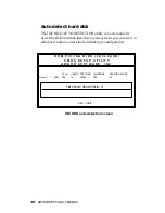
Page 60: ... the chipset s CMOS memory The microprocessor will check this every time you turn your system on and compare this to what it finds as it checks the system This record is required for the system to operate Exit without saving Selecting this option and pressing Enter lets you exit the Setup program without recording any new values or changing old ones ...

Page 61: ...Chapter 4 Driver Installation 53 4 Flat Panel CRT Controller Display Drivers and Utilities This chapter provides information about Driver types and installation C H A P T E R ...

Page 62: ...es not require any special drivers to operate in standard modes The purpose of the enclosed software drivers is to take advantage of the extended features of the CHIPS VGA Flat Panel CRT controller Hardware configuration Some of the high resolution drivers provided in this package will work only in certain system configurations If a driver does not display correctly try the following 1 Change the ...

Page 63: ...rtain about any of these concepts please refer to the DOS or OS 2 user reference guides for more information before you proceed with the installation Before you begin Before you begin the driver software installation you should make backup copies of the Display Driver Diskettes Store the original disks in a safe place Make sure you know the version of the application for which you are installing d...

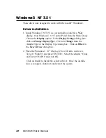
Page 64: ...els list box Select Chips and Tech 65554 PCI new and Click OK Click OK to start the driver installation 3 Once the installation is complete the Change Display Type window will reappear Click on Close to close the window Then the Display Properties window will reappear Click on Apply Restart the system for new settings to take effect 1 Install WindowsÔ 95 as you normally would for a VGA display Cli...

Page 65: ...pull down menu choose Run At the Command Line prompt type A SETUP Press the ENTER key or click OK to begin the installation At this point the setup program locates the directory where Windows is installed For proper operation the drivers must be installed in the Windows subdirectory 3 Press ENTER to complete the installation Once completed you can find the icon Chips CPL under the Control Panel Th...

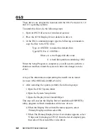
Page 66: ...pleted you will need to perform a shutdown and then restart the system in order for changes to take effect A log of the information output during the install can be found in root OS2 INSTALL DISPLAY LOG 4 After restarting the system perform the following steps 1 Open the OS 2 System folder 2 Open the System Setup folder 3 Open the Display Driver Install Object This step will execute the Display Dr...

Page 67: ...river Installation 59 6 When the installation is complete you will need to shutdown and then restart the system for the changes to take effect Make sure to remove the install diskette before restarting the system ...

Page 68: ...the Display option In the Display Settings dialog box click on Change Display Type Click on Change from the Adapter Type in the Display Type dialog box Click on Other in the Sleect Device dialog box 2 Place the WindowsÔ NT Display Driver Diskette in drive A Type A Winnt3 5 and press ENTER Select the adapter Chips and Tech 65554PCI and click OK Click on Install to install the selected driver Once t...

Page 69: ... Select Device window 2 Place the WindowsÔ NT Display Driver Diskette in drive A In the Select Device window click on Have Disk select Browse and find the NT4 0 driver in the Drive A Winnt4 0 and then click OK The name of the Chips and Technologies Inc Video Controller driver will appear highlighted in the Modules list box Select Chips and Tech 65554 PCI new and Click OK Click OK to start the driv...

Page 70: ...62 SBC 554V 555 User s Manual ...

Page 71: ...dog Timer The SBC 554V 555 is equipped with a watchdog timer that resets the CPU or generates an interrupt if processing comes to a standstill for whatever reason This feature ensures system reliability in industrial stand alone and unmanned environments A P P E N D I X ...

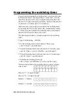
Page 72: ... program should write I O port 80 hex a Hex value The following procedure is a sample program for the watchdog timer Type C DOS Debug ENTER To start watchdog timer and set function Reset type o 444 0 Enter out 444h data 0 To input watchdog timers time out interval of 3 minutes type o 443 83 Enter o 443 0 ENTER out 443h data 83 To input Watchdog timers time out interval of 5 seconds type o 443 05 E...

Reviews: