


User Manual
This document is not allowed to
transmit without ZTE Corporation
’s
permission
©ZTE CORPORATION All rights reserved
29
5
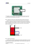
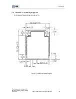
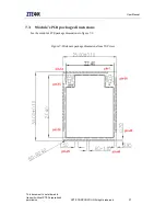
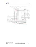
PCB design
5.1
PCB design
1
)
Enough Pad area must be reserved for the module’s grounding pin to guarantee adequate
grounding and avoid interference on the sensitivity.
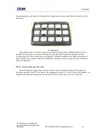
2
)
Copper-clad and wiring are forbidden in the nearby areas of the RF stamp-hole.
3
)
For the convenience of testing and maintenance, it is recommended to drill holes on the PCB to
expose JTAG test points.
4
)
The wiring between the SIM card socket and MCU should be as short as possible to prevent signals
from being affected by long wiring, which might result in the failure of SIM card recognition.