Appendix
App-1
IM 2558A-01EN
3
2
1
4
5
6
7
8
9
10
11
12
13
14
15
16
App
Index
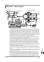
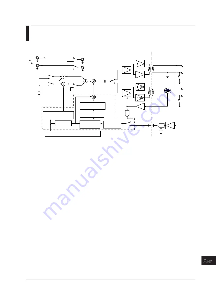
Appendix 1 Block Diagram
Full-wave
rectification
EXT OSC INPUT
I(cos)
Q(sin)
OSC OUTPUT
I(cos)
Q(sin)
ext
int
ext
int
ext
int
Voltage
Current
Voltage amplifier
Current amplifier
Voltage
output
Current
output
Secondary
reference voltage
FG
FG
Reference
voltage
PC
ADC
ADC
I-V converter
CT
Sine wave generation
Phase angle shift
Smoothing
Control (panel control, remote control)
Gain correction
value calculation
Interval average
Level
normalization
Amplitude
control block
Primary side Secondary side
Voltage
Current
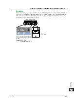
The 2558A consists of a primary side that controls the oscillator output and a secondary side that is
isolated by a transformer. The oscillator signal (the sine wave from the amplitude control block or from
an external signal) is multiplied by the digital signal from the amplitude control block and amplified by
the voltage/current amplifier to produce the voltage and current outputs. In the case of voltage output,
the electrical potential at the LO terminal of the secondary side is used as a reference to detect the
output voltage. Then, the detected value is A-to-D converted, isolated by a photocoupler, and fed back
into the amplitude control block. In the case of current output, a current transformer is used to detect
and isolate the output current. Then, I-V conversion and A-to-D conversion is performed at the primary
electric potential, and the digital signal is fed back into the amplitude control block.
In the amplitude control block, the target output level is set through the panel or remote control.
Smoothing is used to prevent output overshoot and transformer biasing that could occur due to drastic
changes in the output when the setting is changed by a great amount.
The amplifier control block immediately after the output is turned on assumes temporarily that there
are no errors in the amplification factor or input amplitude and provides a coefficient that corresponds
to the setting (after it has been smoothed) to the multiplying DAC. After the operation starts, the
amplitude is adjusted every 0.4 seconds on the basis of the feedback voltage or current signal.
The signal that is fed back to the amplifier control block is fully rectified. Then, level normalization
is used to determine the ratio of the setting to the output amplitude. Next, this ratio is averaged and
weighted over a given interval. The average reflects the amplifier gain and other factors, and is not
directly affected by the setting. This value is then used to calculate the gain correction value to control
the amplitude of the voltage or current output.
As described above, because the 2558A output amplitude is controlled on the basis of waveform
average values, if the output waveform distortion increases due to overloading, the use of a nonlinear
load, or the use of an external signal with large distortion, an error results in the rms output level that is
measured.
On the other hand, if the 2558A is used in a test that checks the excitation current of a transformer or
other device or in a similar application, high reproducibility is achieved because the value depends on
the voltage waveform average.
Though omitted in the block diagram, the value indicated on the OUTPUT display is a weighted
average of the signal fed back to the amplifier control block without any level normalization. To make
it easy to check the output setting, the average duration and display update interval are set to 0.2 s,
which is half the processing time of the amplifier control block. The OUTPUT display and amplifier
control block use the output from the same A-to-D converter. Therefore, if the amplitude is being
controlled stably, the difference between the target value that is calculated digitally and the value on
the OUTPUT display will be about as large as the rounding error (lowest digit ± 1).
Appendix