


CL3/CL1
124
2
Distortion
Input
Frequency
Output Level
Permissible
Range
1 kHz
+22 dBu
0.02 % or below
3
Noise level EIN
Parameters: Short TALKBACK IN with 150
Ω
.
Permissible Range
–64 dBu or below
If the measured value is out of the above permissible range,
con
fi
rm that “measured value – (Gain at 1kHz)
≦
-128” is
obtained.
B. GAIN MIN
1
Gain
Input
Frequency
Input Level
Prescribed
Output Level
Permissible
Range
1 kHz
–16 dBu
+4 dBu
+4±2 dBu
2
Distortion
Input
Frequency
Output Level
Permissible
Range
1 kHz
+22 dBu
0.01 % or below
3
Noise level EIN
Parameters: Short TALKBACK IN with 150
Ω
.
Permissible Range
–80 dBu or below
C. PHANTOM VOLTAGE
With No.2 and No.3 pins of XLR shorted and 10 k
Ω
load
connected between No.2 and No.1 pins, check that the voltage
is as follows when the +48 key is turned on.
Permissible Range
DC 33.6 – 36.1 V
Also, check that discharging starts immediately when the +48
key is turned off.
3. DIGITAL OUT Characteristic Inspection
3-1. 2TR OUT DIGITAL
Parameters: Use system Two.
Input from OMNI IN 1.
A. WORD CLOCK INT48 kHz.
Parameters: Set WORD CLOCK to INT 48 kHz.
1
Gain (2TR OUT DIGITAL)
Input
Frequency
Input Level
Prescribed
Output Level
Permissible
Range
1 kHz
+10 dBu
–20 dBFS
–20±2 dBFS
2
f characteristic (2TR OUT DIGITAL)
Parameters: 1 kHz is used as the reference of the permissible
range.
Input
Frequency
Output Level
Permissible
Range
20 Hz
+10 dBu
–1.0 – 0.5 dB
20 kHz
+10 dBu
–1.0 – 0.5 dB
3
Distortion (2TR OUT DIGITAL)
Input
Frequency
Output Level
Permissible
Range
1 kHz
–2 dBFS
0.002 % or
below
3-2. PLL Operating Range of WORD CLOCK IN
Parameters: Use the System Two.
When measuring the L channel, use OMNI OUT 7
(L).
When measuring the R channel, use OMNI OUT 8
(R).
Select WC IN for WORD CLOCK.
Input from OMNI IN 1.
Use the Dante Controller.
With the PC and Dante PRIMARY terminal of the
main unit connected with a network cable, click
the device label twice.
Click the Device Config tab on the Device View
screen.
A. 48 KHz + 4.1667 % (50 kHz)
Parameters: When checking the WORD CLOCK IN, set the
oscillator frequency to 50 kHz.
Set the Sample Rate column on the Device Con
fi
g
screen as follows.
Pull-up/down: +4.1667 %
1
Distortion (WORD CLOCK IN)
Input
Frequency
Output Level
Permissible
Range
1 kHz
+22 dBu
0.02 % or below
B. 44.1 kHz - 4 % (42.336 kHz)
Parameters: When checking the WORD CLOCK IN, set the
oscillator frequency to 42.336 kHz.
Set the Sample Rate column in the Device Con
fi
g
screen as follows.
Sample Rate: 44 k
Pull-up/down: -4 %
1
Distortion (WORD CLOCK IN)
Input
Frequency
Output Level
Permissible
Range
1 kHz
+22 dBFS
0.02 % or below
Содержание CL3
Страница 7: ...7 CL3 CL1 DIMENSIONS CL3 CL1 648 15 201 130 299 667 839 15 201 130 299 667 Unit mm...
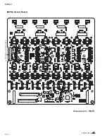
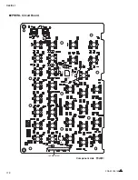
Страница 95: ...95 CL3 CL1 CPU Circuit Board Pattern side to DSP CN101 2NA WY67750 1...
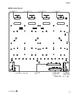
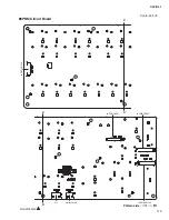
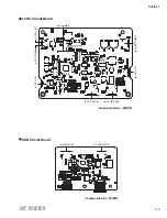
Страница 100: ...CL3 CL1 100 DNTU Circuit Board Component side to DSP CN552 to DANTE MODULE 64CH to DSP CN553 Scale 80 100 2NA WZ20390 5...
Страница 101: ...101 CL3 CL1 DNTU Circuit Board Pattern side Scale 80 100 2NA WZ20390 5...
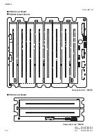
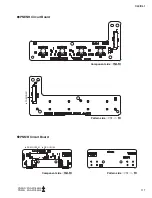
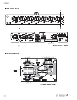
Страница 102: ...CL3 CL1 102 2NA WY63530 FX Circuit Board WR 63 1 Component side Scale 95 100...
Страница 103: ...103 CL3 CL1 2NA WY63530 FX Circuit Board Pattern side Scale 95 100...
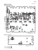
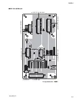
Страница 104: ...CL3 CL1 104 HAAD Circuit Board Component side Scale 90 100 to DSP CN871 to DCMS CN734 2NA WY64340 2...
Страница 105: ...105 CL3 CL1 HAAD Circuit Board Pattern side Scale 90 100 2NA WY64340 2...
Страница 106: ...CL3 CL1 106 Component side DA Circuit Board 1 1 WR 63 1 WR 06 1 WR 63 1 Scale 85 100 2NA WY64350 2...
Страница 107: ...107 CL3 CL1 2NA WY63490 Component side JK Circuit Board WR 63 1...
Страница 109: ...109 CL3 CL1 Component side TBPHN Circuit Board WR 06 1 WR 63 1 2NA WY64360 1...
Страница 110: ...CL3 CL1 110 Component side PN8 Circuit Board to FD8 CN902 or FD8CN CN902 2NA WY53120 2...
Страница 114: ...CL3 CL1 114 PNM Circuit Board Component side Scale 90 100 WR 31 15 1 WR 31 1 C C C C 2NA WY63300 1...
Страница 116: ...CL3 CL1 116 PN2 Circuit Board Component side Pattern side WR 310 1 WR 31 1 WR 1 0 2NA WY63300 1...
Страница 118: ...CL3 CL1 118 Component side PNENL Circuit Board to PN8 CN001 2NA WY53130 1...
Страница 158: ...CL3 CL1 158 UNLOCK WORD CLOCK BNC 1 12 AES EBU OUT test 1KHz OK NG 1 13 MIDI test MIDI 1 14 GPI Test OUT IN...
Страница 160: ...CL3 CL1 160 1 18 LCD Test LCD LCD 1 3 2 9 5 OK NG 1 2 H 3 O X O 4 BOX 5x4...
Страница 178: ...CL3 CL1 178 Status Updating 1 1 6 OK Status Update Done 7 DANTE CONTROLLER Device Status Status Error CL...
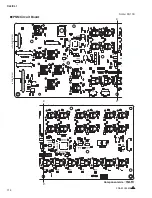
Страница 382: ...7 MBCL CIRCUIT BOARDS A A A A 2NA WY53200 1 MB Circuit Board Component side...
Страница 383: ...MBCL 8 MB Circuit Board DSUB PH CONNECTOR ASSEMBLY B B B B 2NA WY53200 1 Pattern side...


