


ZCU102 Evaluation Board User Guide
68
UG1182 (v1.2) March 20, 2017
Chapter 3:
Board Component Descriptions
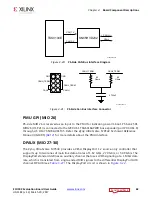
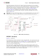
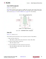
The primary purpose of this clock is to support synchronous protocols (such as CPRI or
OBSAI to perform clock recovery from a user-supplied SFP/SFP+ module) and use the jitter
attenuated recovered clock to drive the reference clock inputs of a GTH transceiver. The
system controller configures the SI5324C in free-run mode (see
). Enabling the jitter attenuation feature requires additional user
programming from the FPGA through the I2C bus. The jitter attenuated clock circuit is
shown in
IMPORTANT:
The Silicon Labs Si5324C U108 pin 1 reset net HDMI_SI5324_RST must be driven High to
enable the device. U108 pin 1 net HDMI_SI5324_RST is connected to FPGA U1 bank 50 pin J12.
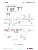
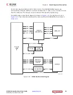
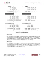
SFP/SFP+ Connector
[
, callout 17]
The ZCU102 board contains a small form-factor pluggable (SFP+) 2x2 quad-connector and
cage assembly that accepts SFP or SFP+ modules.
shows a typical SFP+ module
connector circuitry implementation.
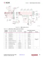
lists the connections between the
connectors and the XCZU9EG MPSoC.
Note that the SFPx_TX_DISABLE_TRANS default 2-pin jumper strapping is Open which
means the SFPx_TX_DISABLE_TRANS net is pulled High, thus disabling the TX output of SFP
module. The open jumper also allows user-FPGA IP to control activation or deactivation of
SFPx_TX_DISABLE_TRANS on each module independently.
X-Ref Target - Figure 3-25
Figure 3-25:
HDMI Interface Clock Recovery


