


WM8580
Production
Data
w
PD, Rev 4.7, March 2009
56
PLL CONFIGURATION
The PLLs perform a configurable frequency multiplication of the input clock signal (f
1
). The
multiplication factor of the PLL (denoted by ‘R’) is variable and is defined by the relationship: R = (f
2
÷
f
1
).
The multiplication factor for each PLL is set using register bits PLLx_N and PLLx_K (refer to Table
47). The multiplication effect of both the N and K multipliers are additive (i.e. if N is configured to
provide a multiplication factor of 8 and K is configured to provide a multiplication factor of 0.192, the
overall multiplication factor is 8 + 0.192 = 8.192).
In order to choose and configure the correct values for PLLx_N and PLLx_K, multiplication factor R
must first be calculated. Once value R is calculated, the value of PLLx_N is the integer (whole
number) value of R, ignoring all digits to the right of the decimal point. For example, if R is calculated
to be 8.196523, PLL_N is simply 8.
Once PLLx_N is calculated, the PLLx_K value is simply the integer value of (2
22
(R-PLLx_N)). For
example, if R is 8.196523 and PLLx_N is 8, PLLx_K is therefore (2
22
(8.196523-8)), which is 824277
(ignoring all digits to the right of the decimal point).
Note:
The PLLs are designed to operate with best performance (shortest lock time and optimum stability)
when f
2
is between 90 and 100MHz and PLLx_N is 8. However, acceptable PLLx_N values lie in the
range 5
≤
PLLx_N
≤
13.
Each PLL has an output divider to allow the f
2
clock signal to be divided to a frequency suitable for
use as the source for the MCLK and CLKOUT outputs, the S/PDIF transmitter and the internal ADC
and DACs. The divider output is configurable and is set by the FREQMODE_A or FREQMODE_B
bits in conjunction with the POSTSCALE_A and POSTSCALE_B bits. Each PLL is also equipped
with a pre-scale divider which offers frequency divide by one or two before the OSCCLK signal is
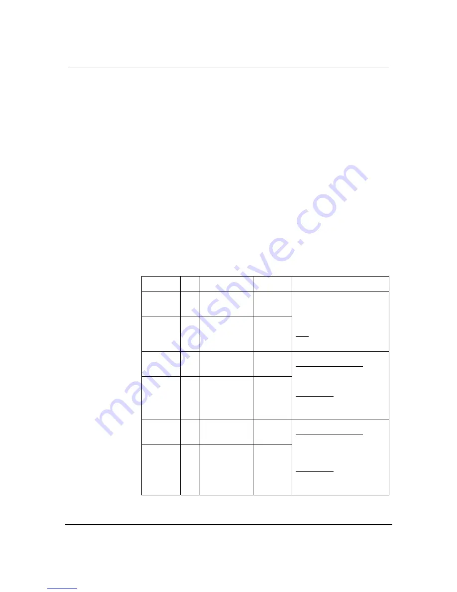
input into the PLL. Please refer to Table 49 for details.
REGISTER
ADDRESS
BIT LABEL DEFAULT
DESCRIPTION
R3
PLLA 4
03h
0 PRESCALE_A
0
R7
PLLB 4
07h
0 PRESCALE_B
0
PLL Pre-scale Divider Select
0 = Divide by 1 (PLL input clock =
oscillator clock)
1 = Divide by 2 (PLL input clock =
oscillator clock
÷
2)
Note: PRESCALE_A must be set to
the same value as PRESCALE_B in
PLL S/PDIF receiver mode.
R3
PLLA 4
03h
4:3 FREQMODE_A
[1:0]
10
R7
PLLB 4
07h
4:3 FREQMODE_B
[1:0]
10
PLL Output Divider Select
PLL S/PDIF Receiver Mode
FREQMODE_A is automatically
controlled. FREQMODE_B is not
used.
PLL User Mode
Used in conjunction with the
POSTSCALE_x bits. Refer to Table
50.
R3
PLLA 4
03h
1 POSTSCALE_A
0
R7
PLLB 4
07h
1 POSTSCALE_B
0
PLL Post-scale Divider Select
PLL S/PDIF Receiver Mode
POSTSCALE_A is used to configure
a 256fs or 128fs PLLACLK,
POSTSCALE_B is not used. Refer
to Table 51.
PLL User Mode
Used in conjunction with the
FREQMODE_x bits. Refer to Table
50.
Table 49 Pre and Post PLL Clock Divider Control
electronic components distributor


