cyber
®
reaction wheel 2
Project planning guide
Revision: 02
Doc. no.: 5022-D060586
en-17
2.2.5.2 B: Application interface
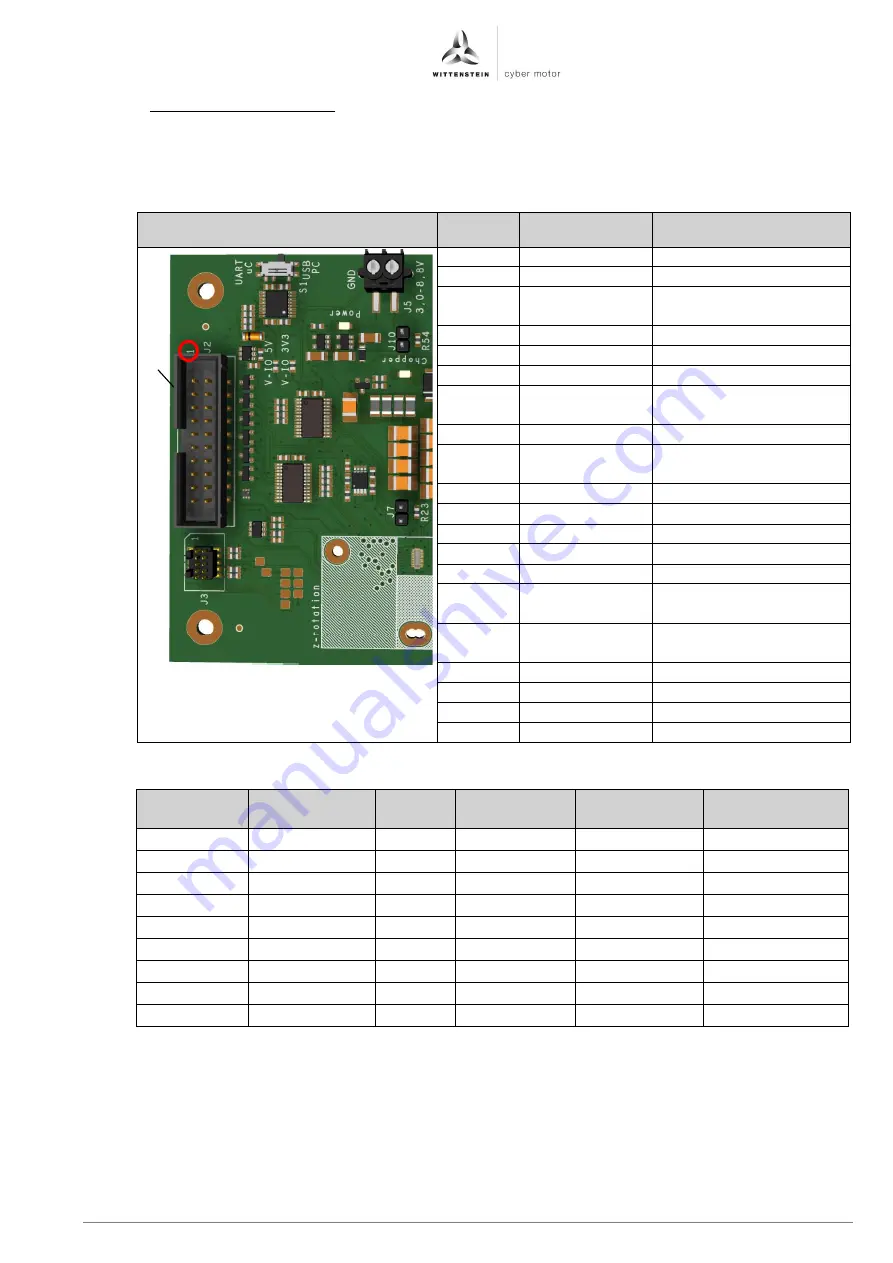
Application interface B, see figure 1.7, is intended for fast and prototypical integration of the
reaction wheel into the target application. Section 3.4 describes how this is to be done.
All signals listed below have an ESD protection diode.
Figure
Pin no.
Signal name
Function
1
GND
Ground reference
2
GND
Ground reference
3
Chopper_Ena
Activation of
underclocking (Out)
4
I2C_SCL
I²C Bus SCL (In)
5
IO_1
User Ouput 1
6
I2C_SDA
I²C Bus SDA (Bi)
7
Reserved
Reserved for CAN Rx
(In)
8
SPI_MOSI
SPI Bus MOSI (In)
9
Reserved
Reserved for CAN Tx
(Out)
10
SPI_MISO
SPI Bus MISO (Out)
11
UART_Tx
Serial interface (Out)
12
SPI_nCS
SPI Bus Chip-Select (In)
13
UART_Rx
Serial interface (In)
14
SPI_CLK
SPI Bus Clock (In)
15
Reserved
Reserved for USB D-
(Bi)
16
Reserved
Reserved for USB D+
(Bi)
17
IO_2
User Ouput 2
18
IO_3
User Input 1
19
V-IO
Logic supply
20
VDD
Reaction wheel supply
Table 11: Pin assignment of application interface, connector B, at the cyber
®
reaction wheel starter kit
Connection
Property
Unit
Minimum
value
Nominal
value
Maximum value
V-IO
Voltage
V
3.0
3.3 / 5.0
5.5
VDD
Voltage
V
3.0
5.0
8.8
Chop_Ena
Voltage
V
Corr. to V-IO
I2C_xx
Voltage
V
Corr. to V-IO
User_IO_x
Voltage
V
3.0
3.3
3.6
CAN_xx
Voltage
V
Corr. to V-IO
SPI_xxx
Voltage
V
Corr. to V-IO
UART_xx
Voltage
V
Corr. to V-IO
USB
Voltage
V
typ. USB
Table 12: Electrical properties of application interface, connector B, at the cyber
®
reaction wheel starter kit
B


