28
32” TFT TV Service Manual
06/03/2006
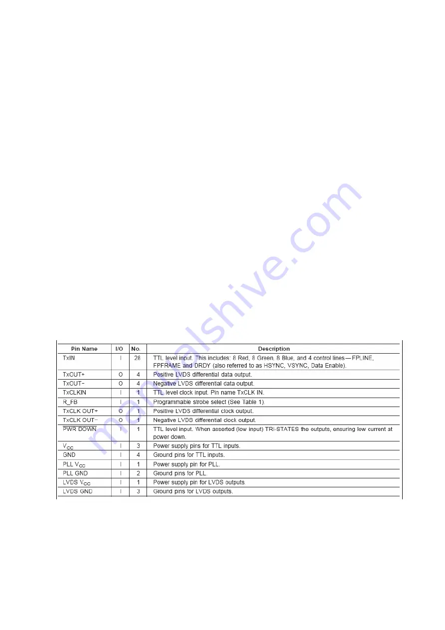
12.18. DS90C385
12.18.1. General Description
The DS90C385 transmitter converts 28 bits of LVCMOS/LVTTL data into four LVDS (Low Voltage
Differential Signaling) data streams. A phase-locked transmit clock is transmitted in parallel with the data
streams over a fifth LVDS link. Every cycle of the transmit clock 28 bits of input data are sampled and
transmitted. At a transmit clock frequency of 85 MHz, 24 bits of RGB data and 3 bits of LCD timing and
control data (FPLINE, FPFRAME, DRDY) are transmitted at a rate of 595 Mbps per LVDS data channel.
Using a 85 MHz clock, the data throughput is 297.5 Mbytes/sec. Also available is the DS90C365 that
converts 21 bits of LVCMOS/LVTTL data into three LVDS (Low Voltage Differential Signaling) data
streams. Both transmitters can be programmed for Rising edge strobe or Falling edge strobe through a
dedicated pin. A Rising edge or Falling edge strobe transmitter will interoperate with a Falling edge strobe
Receiver (DS90CF386/DS90CF366) without any translation logic.
The DS90C385 is also offered in a 64 ball, 0.8mm fine pitch ball grid array (FBGA) package which
provides a 44% reduction in PCB footprint compared to the TSSOP package.
This chipset is an ideal
means to solve EMI and cable size problems associated with wide, high-speed TTL interfaces.
12.18.2. Features
•
20 to 85 MHz shift clock support
•
Best–in–Class Set & Hold Times on TxINPUTs
•
Tx power consumption <130 mW (typ) @85MHz Grayscale
•
Tx Power-down mode <200µW (max)
•
Supports VGA, SVGA, XGA and Single/Dual Pixel SXGA
•
Narrow bus reduces cable size and cost
•
Up to 2.38 Gbps throughput
•
Up to 297.5 Megabytes/sec bandwidth
•
345 mV (typ) swing LVDS devices for low EMI
•
PLL requires no external components
•
Compatible with TIA/EIA-644 LVDS standard
•
Low profile 56-lead or 48-lead TSSOP package
•
DS90C385 also available in a 64 ball, 0.8mm fine pitch ball grid array (FBGA) package
12.18.3. Pinning


