background image

LARA-R2 series - System Integration Manual 

UBX-16010573 - R02 

Objective Specification 

System description 


Page 37 of 148


1.9.1.2


UART AT interface configuration 

The  UART  interface  of  LARA-R2  series  modules  is  available  as  AT  command  interface  with  the  default 
configuration described in Table 10 (for more details and information about further settings, see the

 u-blox AT 

Commands Manual

 [2]). 


Interface 

AT Settings 

Comments 

UART interface 

AT interface: enabled 

AT command interface is enabled by default on the UART physical interface 

AT+IPR=0 

One-shot autobauding enabled by default on the modules 

AT+ICF=3,1 

8N1 frame format enabled by default 

AT&K3 

HW flow control enabled by default 

AT&S1 

DSR line (Circuit 107 in ITU-T V.24) set ON in data mode

6

 and set OFF in command mode

6


AT&D1 

Upon an ON-to-OFF transition of DTR line (Circuit 108/2 in ITU-T V.24), the module (DCE) 
enters online command mode

6

 and issues an OK result code 

AT&C1 

DCD line (Circuit 109 in ITU-T V.24) changes in accordance with the Carrier detect status; 
ON if the Carrier is detected, OFF otherwise 

MUX protocol: disabled 

Multiplexing mode is disabled by default and it can be enabled by AT+CMUX command. 
For more details, see the 

Mux Implementation Application Note

 [21]. 

The following virtual channels are defined: 


Channel 0: control channel 


Channel 1 – 5: AT commands / data connection 


Channel 6: GNSS tunneling

7


Table 10: Default UART AT interface configuration 


1.9.1.3


UART signal behavior 

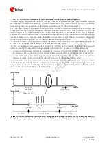
At  the  module  switch-on,  before  the  UART  interface  initialization  (as  described  in  the  power-on  sequence 
reported in Figure 13), each pin is first tri-stated and then is set to its related internal reset state

8

. At the end of 

the  boot  sequence,  the  UART  interface  is  initialized,  the  module  is  by  default  in  active-mode,  and  the  UART 
interface is enabled as AT commands interface. 
The  configuration  and  the  behavior  of  the  UART  signals  after  the  boot  sequence  are  described  below.  See 
section 1.4 for definition and description of module operating modes referred to in this section. 
 

RXD signal behavior 

The  module  data  output  line  (

RXD

)  is  set  by  default  to  the  OFF  state  (high  level)  at  UART  initialization.  The 

module holds 

RXD

 in the OFF state until the module does not transmit some data. 


TXD signal behavior 

The module data input line (

TXD

) is set by default to the OFF state (high level) at UART initialization. The 

TXD


line is then held by the module in the OFF state if the line is not activated by the DTE: an active pull-up is enabled 
inside the module on the 

TXD

 input. 


6

 See the

 u-blox AT Commands Manual

 [2] for the definition of the command mode, data mode, and online command mode 

7

 Not supported by “02” product versions 

8

 Refer to the pin description table in the

 LARA-R2 series


Data Sheet 

[1]

.


Содержание LARA-R2 series

Страница 1: ...the system integration of LARA R2 series multi mode cellular modules These modules are a complete cost efficient and performance optimized LTE Cat 1 2G multi mode solution covering up to three LTE ban...

Страница 2: ...00 UBX 16024242 u blox reserves all rights to this document and the information contained herein Products names logos and designs described herein may in whole or in part be subject to intellectual pr...

Страница 3: ...ovides the necessary information to successfully design in and configure these u blox cellular modules This manual has a modular structure It is not necessary to read it from the beginning to the end...

Страница 4: ...election 31 1 7 Antenna interface 32 1 7 1 Antenna RF interfaces ANT1 ANT2 32 1 7 2 Antenna detection interface ANT_DET 34 1 8 SIM interface 34 1 8 1 SIM card interface 34 1 8 2 SIM card detection int...

Страница 5: ..._ON 82 2 3 2 Module reset RESET_N 83 2 3 3 Module host configuration selection 84 2 4 Antenna interface 85 2 4 1 Antenna RF interface ANT1 ANT2 85 2 4 2 Antenna detection interface ANT_DET 92 2 5 SIM...

Страница 6: ...ication approval overview 130 4 2 US Federal Communications Commission notice 131 4 2 1 Safety warnings review the structure 131 4 2 2 Declaration of conformity 131 4 2 3 Modifications 131 4 3 Industr...

Страница 7: ...g term availability and scalability of LTE networks With a range of interface options and an integrated IP stack the modules are designed to support a wide range of data centric applications The uniqu...

Страница 8: ...1 30 dBm for DCS band EDGE 8 PSK Power Class Power Class E2 27 dBm for E GSM band Power Class E2 26 dBm for DCS band Data rate LTE category 1 up to 10 3 Mb s DL 5 2 Mb s UL Data Rate2 GPRS multi slot...

Страница 9: ...ANT1 of the module via power amplifier PA SAW band pass filters band specific duplexer and antenna switch Dual receiving paths are implemented according to LTE Receiver Diversity radio technology sup...

Страница 10: ...paths Memory interface controller Dedicated peripheral blocks for control of the USB SIM and generic digital interfaces Interfaces to RF transceiver ASIC Memory system which includes NAND flash and L...

Страница 11: ...15 I Power on input Internal 10 k pull up resistor to V_BCKP See section 1 6 1 for functional description See section 2 3 1 for external circuit design in RESET_N 18 I External reset input Internal 1...

Страница 12: ...te by u blox EasyFlash tool and diagnostic Internal active pull up to V_INT Test Point and series 0 for diagnostic access recommended See section 1 9 1 for functional description See section 2 6 1 for...

Страница 13: ...M Pull up or pull down resistors and external series resistors as required by the USB 2 0 specifications 9 are part of the USB pin driver and need not be provided externally If the USB interface is no...

Страница 14: ...l circuit design in SDIO_CMD 46 I O SDIO command Not supported by 02 product versions SDIO interface for communication with u blox Wi Fi module See section 1 9 5 for functional description See section...

Страница 15: ...O with alternatively configurable functions See section 1 12 for functional description See section 2 8 for external circuit design in GPIO4 25 I O GPIO 1 8 V GPIO with alternatively configurable func...

Страница 16: ...mode by removing VCC supply Idle Module is switched on with application interfaces temporarily disabled or suspended the module is temporarily not ready to communicate with an external device by means...

Страница 17: ...sections 1 5 1 3 1 9 1 4 and the u blox AT Commands Manual 2 When a data or voice connection is initiated the module enters connected mode from active mode Connected mode is suspended if Tx Rx data is...

Страница 18: ...d in section 1 5 1 2 to the low current consumption during low power idle mode with power saving enabled as described in section 1 5 1 4 LARA R211 modules provide separate supply inputs over the three...

Страница 19: ...bove VCC extended operating range is not recommended and may affect device reliability VCC average current Support with adequate margin the highest averaged VCC current consumption value in connected...

Страница 20: ...te less high than the one in the low bands due to 3GPP transmitter output power specifications During a GSM call current consumption is not so significantly high in receiving or in monitor bursts and...

Страница 21: ...bursts with a periodicity of 4 615 ms width of 1 frame 8 slots bursts so with a 1 2 duty cycle according to 2G TDMA If the module is in GPRS connected mode in the 1800 or 1900 MHz bands the current c...

Страница 22: ...eaks since transmission and reception are continuously enabled in FDD In the worst scenario corresponding to a continuous transmission and reception at maximum output power approximately 250 mW or 24...

Страница 23: ...Hz used in active mode The time period between two paging block receptions is defined by the network This is the paging period parameter fixed by the base station through broadcast channel sent to all...

Страница 24: ...ncy is used Figure 9 illustrates a typical example of the module current consumption profile when power saving is disabled In such case the module is registered with the network and while active mode...

Страница 25: ...its valid range specified in the Input characteristics of Supply Power pins table in LARA R2 series Data Sheet 1 The RTC can be supplied from an external back up battery through the V_BCKP when the m...

Страница 26: ...interfaces of the cellular module as described in Figure 11 The output of this regulator is enabled when the module is switched on and it is disabled when the module is switched off Baseband Processor...

Страница 27: ...pplication releases the PWR_ON input pin from the low logic level after that the VCC supply voltage stabilizes at its proper nominal value within the operating range When the LARA R2 series modules ar...

Страница 28: ...ET_N V_INT Internal Reset System State BB Pads State Internal Reset Operational Operational Tristate Floating Internal Reset OFF ON Start of interface configuration Module interfaces are configured St...

Страница 29: ...east until the end of the modules internal power off sequence which occurs when the generic digital interfaces supply output V_INT is switched off by the module An abrupt hardware shutdown occurs on L...

Страница 30: ...except the RTC supply V_BCKP Then the module remains in power off mode as long as a switch on event does not occur e g applying a proper low level to the PWR_ON input or applying a proper low level to...

Страница 31: ...le by forcing a low level on the RESET_N input during modules normal operation the RESET_N line should be set low only if reset or shutdown via AT commands fails or if the module does not provide a re...

Страница 32: ...RA R2 series Data Sheet 1 The required frequency range of the antenna connected to ANT1 port depends on the operating bands of the used cellular module and the used mobile network Return Loss S11 10 d...

Страница 33: ...he Air OTA radiated performance requirements as the TIS specified by applicable related certification schemes Table 8 Summary of secondary Rx antenna RF interface ANT2 requirements Item Requirements R...

Страница 34: ...connected SIM card or chip Both 1 8 V and 3 V SIM types are supported activation and deactivation with automatic voltage switch from 1 8 V to 3 V is implemented according to ISO IEC 7816 3 specificat...

Страница 35: ...The UART interface is a 9 wire 1 8 V unbalanced asynchronous serial interface available on all the LARA R2 series modules supporting AT command mode 5 Data mode and Online command mode 5 Multiplexer p...

Страница 36: ...on autobauding is enabled by default The following baud rates can be configured by AT command see u blox AT Commands Manual 2 IPR 9600 b s 19200 b s 38400 b s 57600 b s 115200 b s default value when o...

Страница 37: ...efined Channel 0 control channel Channel 1 5 AT commands data connection Channel 6 GNSS tunneling7 Table 10 Default UART AT interface configuration 1 9 1 3 UART signal behavior At the module switch on...

Страница 38: ...he OFF state if the line is not activated by the DTE an active pull up is enabled inside the module on the RTS input If the HW flow control is enabled as it is by default the module monitors the RTS l...

Страница 39: ...module sets the DCD line to the ON state then answers with a CONNECT to confirm the ATD 99 command The DCD ON is not related to the context activation but with the data mode Circuit Switched Data cal...

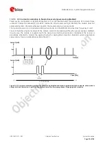
Страница 40: ...rvice For SMS arrival if several events coincidently occur or in quick succession each event independently triggers the RI line although the line will not be deactivated between each event As a result...

Страница 41: ...idle mode and wake up 0 Enabled AT K3 ON ON or OFF Data sent by the DTE are correctly received by the module Data sent by the module is correctly received by the DTE 0 Enabled AT K3 OFF ON or OFF Data...

Страница 42: ...on 1 5 1 4 or other activities If the module needs to transmit some data e g URC the UART is temporarily enabled to send data If the DTE send data with HW flow control disabled the first character sen...

Страница 43: ...le but it wakes up to active mode according to any required activity related to the network e g for the periodic paging reception described in section 1 5 1 4 or for any other required RF transmission...

Страница 44: ...ation is active and the timeout from last data received to idle mode start is set to 2000 frames AT UPSV 1 2000 Hardware flow control is disabled Figure 20 shows the case where the module UART is disa...

Страница 45: ...ording to the AT UPSV settings To set the AT UPSV 1 AT UPSV 2 or AT UPSV 3 configuration over the USB interface the autobauding must be previously disabled on the UART by the IPR AT command over the u...

Страница 46: ...DET input the VUSB_DET senses the USB supply voltage and absorbs few microamperes The USB interface is controlled and operated with AT commands according to 3GPP TS 27 007 6 3GPP TS 27 005 7 u blox AT...

Страница 47: ...bstract Control Model EndPoint Transfer Interrupt Interface 1 Data EndPoint Transfer Bulk EndPoint Transfer Bulk Function AT and Data Interface 2 Abstract Control Model EndPoint Transfer Interrupt Int...

Страница 48: ...USB is suspended and a power saving configuration is enabled by the AT UPSV command the module automatically enters the low power idle mode whenever possible but it wakes up to active mode according...

Страница 49: ...T feature see 1 14 13 and Firmware update application note 23 FW upgrades by means of the u blox EasyFlash tool see the Firmware update application note 23 Trace log capture diagnostic purpose The HSI...

Страница 50: ...T commands via the UART or USB serial interface of the cellular module allows a fully control of the GNSS receiver from any host processor The modules feature embedded GNSS aiding that is a set of spe...

Страница 51: ...eakdown with either a hot start or a warm start depending on the duration of the GNSS receiver VCC outage and to maintain the configuration settings saved in the backup RAM 1 9 5 SDIO interface Secure...

Страница 52: ...is set high low with a 50 duty cycle high for 16 clock cycles low for 16 clock cycles according to the 32 clock cycles frame length The I 2 S interface can be alternatively set in different roles by...

Страница 53: ...ble disable the supply of u blox GNSS receiver connected to the cellular module GPIO1 GPIO4 GNSS data ready14 Sense when u blox GNSS receiver connected to the module is ready for sending data by the D...

Страница 54: ...n application board and diagnostic circuit on antenna assembly design in guidelines 1 14 3 Jamming detection Congestion detection i e jamming detection is not supported by 02 product versions In real...

Страница 55: ...ovide embedded File Transfer Protocol FTP services Files are read and stored in the local file system of the module FTP files can also be transferred using FTP Direct Link FTP download data coming fro...

Страница 56: ...s of the products For a complete list of supported configurations and settings see the u blox AT Commands Manual 2 Settings Value Meaning Certificates validation level Level 0 The server certificate w...

Страница 57: ...ch a cellular module provides a SIM with access to the data bearers supported by the network With the BIP for Over the Air SIM provisioning the data transfer from and to the SIM uses either an already...

Страница 58: ...pplications Positioning through cellular information CellLocate u blox CellLocate enables the device position estimation based on the parameters of the mobile network cells visible to the specific dev...

Страница 59: ...eiver or the position estimated from CellLocate The choice depends on which positioning method provides the best and fastest solution according to the user configuration exploiting the benefit of havi...

Страница 60: ...r cellular only operation 1 14 13 Firmware upgrade Over AT FOAT This feature allows upgrading the module firmware over USB UART serial interfaces using AT commands The UFWUPD AT command triggers a reb...

Страница 61: ...ined thresholds to identify the actual working temperature range Temperature measurement is done inside the module the measured value could be different from the environmental temperature Ta Warning a...

Страница 62: ...Shut the device down Yes No Yes Yes No No No Yes Send shutdown notification Feature enabled full logic or indication only IF Full Logic Enabled Feature disabled no action Temperature is within normal...

Страница 63: ...the module automatically enters the low power idle mode whenever possible reducing current consumption see section 1 5 1 4 LARA R2 series Data Sheet 1 During the low power idle mode the module is tem...

Страница 64: ...design is required to guarantee SIM card functionality and compliance with applicable conformance standards reducing also the risk of RF coupling Carefully follow the suggestions provided in section...

Страница 65: ...s VCC operating supply voltage The use of switching step down provides the best power efficiency for the overall application and minimizes current drawn from the main supply source See sections 2 2 1...

Страница 66: ...ve providing application circuit design in compliant with the module VCC requirements summarized in Table 6 2 2 1 2 Guidelines for VCC supply circuit design using a switching regulator The use of a sw...

Страница 67: ...Ceramic X7R 0402 10 16 V GRM155R71C103KA01 Murata C3 680 pF Capacitor Ceramic X7R 0402 10 16 V GRM155R71H681KA01 Murata C4 22 pF Capacitor Ceramic C0G 0402 5 25 V GRM1555C1H220JZ01 Murata C5 10 nF Cap...

Страница 68: ...1E226KE15 Murata C2 100 F Capacitor Tantalum B_SIZE 20 6 3V 15m T520B107M006ATE015 Kemet C3 5 6 nF Capacitor Ceramic X7R 0402 10 50 V GRM155R71H562KA88 Murata C4 6 8 nF Capacitor Ceramic X7R 0402 10 5...

Страница 69: ...ation of the regulator Figure 28 and the components listed in Table 21 show an example of a high reliability power supply circuit where the VCC module supply is provided by an LDO linear regulator cap...

Страница 70: ...ly below the maximum limit of the module VCC normal operating range e g 4 1 V as in the circuit described in Figure 29 and Table 22 This reduces the power on the linear regulator and improves the whol...

Страница 71: ...le Li Ion battery with its output circuit must be capable of avoiding a VCC voltage drop below the operating range summarized in Table 6 during transmit bursts 2 2 1 5 Guidelines for VCC supply circui...

Страница 72: ...apacitor e g Murata GRM155R71C103K to filter digital logic noise from clocks and data sources 100 nF capacitor e g Murata GRM155R61C104K to filter digital logic noise from clocks and data sources A su...

Страница 73: ...Description Part Number Manufacturer C1 330 F Capacitor Tantalum D_SIZE 6 3 V 45 m T520D337M006ATE045 KEMET C2 10 nF Capacitor Ceramic X7R 0402 10 16 V GRM155R71C103KA01 Murata C3 100 nF Capacitor Cer...

Страница 74: ...LARA R2 series 52 VCC 53 VCC 51 VCC USB Supply C3 R4 U1 IUSB IAC IEND TPRG SD VIN VINSNS MODE ISEL C2 C1 5V TH GND VOUT VOSNS VREF R1 R2 R3 Li Ion Li Pol Battery Pack D1 B1 C4 Li Ion Li Polymer Batter...

Страница 75: ...ram Figure 34 and the components listed in Table 26 provide an application circuit example where the MPS MP2617 switching charger regulator with integrated power path management function provides the...

Страница 76: ...T C4 R1 R2 D1 Li Ion Li Pol Battery Pack B1 C5 Li Ion Li Polymer Battery Charger Regulator with Power Path Managment VCC C3 C6 L1 BST D2 VLIM R4 R5 C7 C8 C9 C14 C15 Figure 34 Li Ion or Li Polymer batt...

Страница 77: ...ample less than 50 m to minimize voltage drops Adequate maximum Drain current see LARA R2 series Data Sheet 1 for module consumption figures Low leakage current to minimize the current consumption C3...

Страница 78: ...s in the worst case Shielding of switching DC DC converter circuit or at least the use of shielded inductors for the switching DC DC converter may be considered since all switching power supplies may...

Страница 79: ...t the RTC run for 1 minute after VCC removal b using a 70 mF capacitor to let RTC run for 10 hours after VCC removal c using a non rechargeable battery Reference Description Part Number Manufacturer C...

Страница 80: ...rding the application circuit with a u blox GNSS receiver The internal regulator for V_BCKP is optimized for low leakage current and very light loads Do not apply loads which might exceed the limit fo...

Страница 81: ...exceed the limit for maximum available current from V_INT supply see the LARA R2 series Data Sheet 1 as this can cause malfunctions in internal circuitry Since the V_INT supply is generated by an inte...

Страница 82: ...put is suitable to drive the PWR_ON input from an application processor as the pin is equipped with an internal active pull up resistor to the V_BCKP supply as described in Figure 37 A compatible push...

Страница 83: ...as it is equipped with an internal pull up to V_BCKP supply as described in Figure 38 A compatible push pull output of an application processor can also be used In any case take care to set the proper...

Страница 84: ...tion Manual Do not apply voltage to HOST_SELECT pin before the switch on of its supply source V_INT to avoid latch up of circuits and allow a proper boot of the module If the external signal connected...

Страница 85: ...mounted o The radiation performance mainly depends on the antennas It is required to select antennas with optimal radiating performance in the operating bands o RF cables should be carefully selected...

Страница 86: ...t antennas providing appropriate gain figure i e combined antenna directivity and efficiency figure so that the electromagnetic field radiation intensity do not exceed the regulatory limits specified...

Страница 87: ...35 um 35 um 35 um 35 um 270 um 270 um 760 um L1 Copper L3 Copper L2 Copper L4 Copper FR 4 dielectric FR 4 dielectric FR 4 dielectric 380 um 500 um 500 um Figure 40 Example of 50 coplanar waveguide tra...

Страница 88: ...ayer to buried layer dielectric thickness is below 200 m to reduce parasitic capacitance to ground The transmission line width and spacing to GND must be uniform and routed as smoothly as possible avo...

Страница 89: ...nd plane of the application PCB can be reduced down to a minimum size that must be similar to one quarter of wavelength of the minimum frequency that has to be radiated As numerical example Frequency...

Страница 90: ...2 mm Table 31 Examples of internal surface mount antennas Table 32 lists some examples of possible internal off board PCB type antennas with cable and connector Manufacturer Part Number Product Name...

Страница 91: ...ion antenna waterproof IP67 rated with cable and SMA M 698 960 MHz 1710 2170 MHz 2400 2700 MHz 205 8 x 58 x 12 4 mm Laird Tech TRA6927M3PW 001 GSM WCDMA LTE screw mount antenna with N type F 698 960 M...

Страница 92: ...J02 Murata R1 10 k Resistor 0402 1 0 063 W RK73H1ETTP1002F KOA Speer J1 J2 SMA Connector 50 Through Hole Jack SMA6251A1 3GT50G 50 Amphenol C4 C5 22 pF Capacitor Ceramic C0G 0402 5 25 V GRM1555C1H220J...

Страница 93: ...ns that that the antenna is not connected or the RF cable is broken Reported values below the measurement range minimum limit 1 k highlights a short to GND at antenna or along the RF cable Measurement...

Страница 94: ...are suitable for applications requiring a change of SIM card during the product lifetime A SIM card holder can have 6 or 8 positions if a mechanical card presence detector is not provided or it can h...

Страница 95: ...ction e g Tyco Electronics PESD0402 140 on each externally accessible SIM line close to each related pad of the SIM connector ESD sensitivity rating of the SIM interface pins is 1 kV HBM so that accor...

Страница 96: ...each SIM line VSIM SIM_CLK SIM_IO SIM_RST to prevent RF coupling especially in case the RF antenna is placed closer than 10 30 cm from the SIM card holder Limit capacitance and series resistance on ea...

Страница 97: ...d pad of the SIM connector to prevent RF coupling especially in case the RF antenna is placed closer than 10 30 cm from the SIM card holder Provide a low capacitance i e less than 10 pF ESD protection...

Страница 98: ...tch between more than 2 SIM a circuit similar to the one described in Figure 47 can be implemented in case of 4 SIM circuit using proper 4 throw switch instead of the suggested 2 throw switches Follow...

Страница 99: ...cards with SIM detection not implemented 2 5 1 2 Guidelines for SIM layout design The layout of the SIM card interface lines VSIM SIM_CLK SIM_IO SIM_RST may be critical if the SIM card is placed far...

Страница 100: ...8 V DTE If a 3 0 V Application Processor DTE is used then it is recommended to connect the 1 8 V UART interface of the module DCE by means of appropriate unidirectional voltage translators using the...

Страница 101: ...Processor DTE is used then it is recommended to connect the 1 8 V UART interface of the module DCE by means of appropriate unidirectional voltage translators using the module V_INT output as 1 8 V sup...

Страница 102: ...CE serial communication 1 8 V DTE If a 3 0 V Application Processor DTE is used then it is recommended to connect the 1 8 V UART interface of the module DCE by means of appropriate unidirectional volta...

Страница 103: ...series 1 8V DCE 12 TXD 9 DTR 13 RXD 10 RTS 11 CTS 6 DSR 7 RI 8 DCD GND 0 TP 0 TP 0 TP TP Figure 54 UART interface application circuit with partial V 24 link 3 wire in the DTE DCE serial communication...

Страница 104: ...lines only is not recommended During command mode the DTE must send to the module a wake up character or a dummy AT before each command line see section 1 9 1 4 for the complete description but during...

Страница 105: ...e point on the line connected to this pin as described in Figure 56 and Table 43 The USB interface pins ESD sensitivity rating is 1 kV Human Body Model according to JESD22 A114F Higher protection leve...

Страница 106: ...ce ZCM is as close as possible to 30 Consider design rules for USB_D USB_D similar to RF transmission lines being them coupled differential micro strip or buried stripline avoid any stubs abrupt chang...

Страница 107: ...ed on the same PCB of the LARA R2 series module without using connectors cables as described in Figure 59 The modules include also the HOST_SELECT pin to select the module host application processor c...

Страница 108: ...r sensitive analog inputs since the signals can cause the radiation of some harmonics of the digital data frequency Figure 40 and Figure 41 provide two examples of proper 50 coplanar waveguide designs...

Страница 109: ...values e g 3 0 V Connect the DDC I 2 C pull ups to the V_INT 1 8 V supply source or another 1 8 V supply source enabled after V_INT e g as the GNSS 1 8 V supply present in Figure 60 application circu...

Страница 110: ...of the cellular module is connected to the V_BCKP backup supply input pin of the GNSS receiver to provide the supply for the GNSS real time clock and backup RAM when the VCC supply of the cellular mo...

Страница 111: ...l filtering may be needed to properly supply an external LNA depending on the characteristics of the used LNA adding a series ferrite bead and a bypass capacitor e g the Murata BLM15HD182SN1 ferrite b...

Страница 112: ...V GNSS receiver u blox GNSS 3 0 V receiver 24 GPIO3 1V8 B1 A1 GND U3 B2 A2 VCCB VCCA Unidirectional Voltage Translator C4 C5 3V0 TxD1 R1 IN OUT GNSS LDO Regulator SHDNn R2 VMAIN 3V0 U1 23 GPIO2 26 SD...

Страница 113: ...for SDIO interface circuit design will be described in detail in a successive release of the System Integration Manual Do not apply voltage to any SDIO interface pin before the switch on of SDIO inte...

Страница 114: ...te i e synch signal frequency configurable by AT UI2S I2S_sample_rate parameter o 8 kHz o 11 025 kHz o 12 kHz o 16 kHz o 22 05 kHz o 24 kHz o 32 kHz o 44 1 kHz o 48 kHz The same serial clock frequency...

Страница 115: ...terface which can concurrently communicate with other I 2 C devices and control an external audio codec The V_INT output supplies the external audio codec defining proper digital interfaces voltage le...

Страница 116: ...witch on ESD sensitivity rating of I 2 S interface pins is 1 kV Human Body Model according to JESD22 A114 Higher protection level could be required if the lines are externally accessible and it can be...

Страница 117: ...ines for the downlink path speaker receiver are the following The physical width of the audio output lines on the application board must be wide enough to minimize series resistance since the lines ar...

Страница 118: ...90KRKT Lite on Technology Corporation T1 NPN BJT Transistor BC847 Infineon Table 48 Components for network indication application circuit Use transistors with at least an integrated resistor in the ba...

Страница 119: ...urce of radiated energy including digital circuits that can radiate some digital frequency harmonics which can produce Electro Magnetic Interference affecting module RF and analog parts circuits perfo...

Страница 120: ...requirements Foot print Top View K M1 M1 M2 E H J E B K G H J D A D O O L N L I F1 F2 G G H H H G G Pin 1 ANT1 ANT2 K M1 M1 M2 E H J E B K G H J D A D O O L N L I F1 F2 G G H H H G G ANT1 ANT2 Pin 1...

Страница 121: ...circuitry for a given operating ambient temperature This improves the device long term reliability in particular for applications operating at high ambient temperature Recommended hardware techniques...

Страница 122: ...electromagnetic field radiates If the device implements an integral antenna the enclosure port is defined as all insulating and conductive surfaces housing the device If the device implements a remov...

Страница 123: ...4 45 VBUS 17 VUSB_DET 100nF 62 ANT2 59 ANT_DET 10k Connector 27pF ESD Secondary Cellular Antenna 33pF 82nH 82nH 56 Connector Primary Cellular Antenna 33pF ANT1 GND 16 GPIO1 3V8 Network Indicator RSVD...

Страница 124: ...tly connected to all the UART pins of the LARA R2 series modules TXD RXD DTR DCD for diagnostic purpose in particular providing a 0 series jumper on each line to detach each UART pin of the module fro...

Страница 125: ...mmon mode and should not be routed close to any RF line part HSIC traces has to be designed as 50 nominal characteristic impedance transmission lines Keep the SDIO traces short avoid stubs avoid coupl...

Страница 126: ...e manufacturing area The main principle of an EPA is that there are no highly charging materials near ESD sensitive electronics all conductive materials are grounded workers are grounded and charge bu...

Страница 127: ...7530 Guidelines for temperature profiling for mass soldering reflow and wave processes published 2001 Reflow profiles are to be selected according to the following recommendations Failure to observe...

Страница 128: ...3 3 Optical inspection After soldering the LARA R2 series modules inspect the modules optically to verify that the module is properly aligned and centered 3 3 4 Cleaning Cleaning the soldered modules...

Страница 129: ...The RF shields do not provide 100 protection for the module from coating liquids with low viscosity therefore care is required in applying the coating Conformal Coating of the module will void the wa...

Страница 130: ...cation schemes the application device that integrates the modules must be approved under all the certification schemes required by the specific application device to be deployed in the market The requ...

Страница 131: ...this equipment complies with FCC radiation exposure limits prescribed for an uncontrolled environment for fixed and mobile use conditions This equipment should be installed and operated with a minimu...

Страница 132: ...ion between the equipment and receiver o Connect the equipment into an outlet on a circuit different from that to which the receiver is connected o Consultant the dealer or an experienced radio TV tec...

Страница 133: ...tions incorporating the LARA R2 series modules are required to have their final product certified and apply for their own Industry Canada Certificate related to the specific portable device This is ma...

Страница 134: ...atisfy the essential requirements of the 1999 5 EC Directive the modules are compliant with the following standards Radio Frequency spectrum use R TTE art 3 2 o EN 301 511 o EN 301 908 1 o EN 301 908...

Страница 135: ...ates typical automatic test equipment ATE in a production line The following typical tests are among the production tests Digital self test firmware download Flash firmware verification IMEI programmi...

Страница 136: ...perform RF performance tests see the following section 5 2 2 for details 5 2 1 Go No go tests for integrated devices A Go No go test is typically to compare the signal quality with a Golden Device in...

Страница 137: ...wer ignoring cellular signaling protocol This emission can generate interference that can be prohibited by law in some countries The use of this feature is intended for testing purpose in controlled e...

Страница 138: ...VUSB_DET GND USB _ D USB _ D RSVD GND GPIO2 GPIO3 SDA SCL GPIO4 GND GND GND GND VCC VCC RSVD I2S_TXD I2S_CLK SIM_CLK SIM_IO VSIM SIM_DET VCC SIM_RST I2S_RXD I2S_WA GND GND GND GND GND GND GND GND GND...

Страница 139: ...ule SARA cellular module Nested application board TOBY cellular module Figure 72 Nested design concept description SARA LARA LISA and TOBY modules alternatively mounted on the same PCB A different top...

Страница 140: ...ummary of SARA U2 and LARA R2 series modules interfaces Figure 74 summarizes the LTE 3G and 2G operating frequency bands of SARA U2 and LARA R2 series modules SARA U260 SARA U270 SARA U280 SARA U201 8...

Страница 141: ...onal difference 13 RXD UART Data Output 1 8 V Driver strength 6 mA RXD UART Data Output 1 8 V Driver strength 6 mA No functional difference 14 GND Ground GND Ground 15 PWR_ON Power on Input No interna...

Страница 142: ...put SIM_RST SIM Reset Output No functional difference 41 VSIM SIM Supply Output VSIM SIM Supply Output No functional difference 42 SIM_DET 1 8V SIM Detection SIM_DET 1 8 V GPIO settable as SIM Detecti...

Страница 143: ...CLK 44 45 VBUS 17 VUSB_DET 100nF 62 ANT_DET ANT2 59 GND ANT_DET 10k Connector 27pF ESD Secondary Cellular Antenna 33pF 82nH 82nH 56 Connector Primary Cellular Antenna 33pF ANT ANT1 V_INT BCLK LRCLK Au...

Страница 144: ...Signal Processing DTE Data Terminal Equipment EDGE Enhanced Data rates for GSM Evolution EMC Electro magnetic Compatibility EMI Electro magnetic Interference ESD Electro static Discharge ESR Equivalen...

Страница 145: ...cure Digital Input Output SDN IN PCN Sample Delivery Note Information Note Product Change Notification SIM Subscriber Identification Module SMS Short Message Service SMTP Simple Mail Transfer Protocol...

Страница 146: ...ce specification Radio transmission and reception Part 2 Implementation Conformance Statement ICS 15 3GPP TS 36 523 2 Evolved Universal Terrestrial Radio Access E UTRA and Evolved Packet Core EPC User...

Страница 147: ...RA R2 series System Integration Manual UBX 16010573 R02 Objective Specification Revision history Page 147 of 148 Revision history Revision Date Name Status Comments R01 20 Sep 2016 sses Initial releas...

Страница 148: ..._ap u blox com Regional Office China Beijing Phone 86 10 68 133 545 E mail info_cn u blox com Support support_cn u blox com Regional Office China Chongqing Phone 86 23 6815 1588 E mail info_cn u blox...

Отзывы: