


LARA-R2 series - System Integration Manual
UBX-16010573 - R02
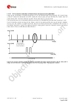
Objective Specification
System description
Page 13 of 148
Function
Pin Name
Pin No
I/O
Description
Remarks
USB
VUSB_DET
17
I
USB detect input
VBUS (5 V typical) USB supply generated by the host must
be connected to this input pin to enable the USB interface.
If the USB interface is not used by the Application Processor,
Test-Point for diagnostic / FW update access is recommended
See section 1.9.2 for functional description.
See section 2.6.2 for external circuit design-in.
USB_D-
28
I/O
USB Data Line D-
USB interface for AT commands, data communication,
FOAT, FW update by u-blox EasyFlash tool and diagnostic.
90
nominal differential impedance (Z
0
)
30
nominal common mode impedance (Z
CM
)
Pull-up or pull-down resistors and external series resistors as
required by the
USB 2.0 specifications
[9] are part of the
USB pin driver and need not be provided externally.
If the USB interface is not used by the Application Processor,
Test-Point for diagnostic / FW update access is recommended
See section 1.9.2 for functional description.
See section 2.6.2 for external circuit design-in.
USB_D+
29
I/O
USB Data Line D+
USB interface for AT commands, data communication,
FOAT, FW update by u-blox EasyFlash tool and diagnostic.
90
nominal differential impedance (Z
0
)
30
nominal common mode impedance (Z
CM
)
Pull-up or pull-down resistors and external series resistors as
required by the
USB 2.0 specifications
[9] are part of the
USB pin driver and need not be provided externally.
If the USB interface is not used by the Application Processor,
Test-Point for diagnostic / FW update access is recommended
See section 1.9.2 for functional description.
See section 2.6.2 for external circuit design-in.
HSIC
HSIC_DATA
99
I/O
HSIC USB data line
Not supported by “02” product versions.
USB High-Speed Inter-Chip compliant interface for AT
commands, data communication, FOAT, FW update by u-
blox EasyFlash tool and diagnostic.
50
nominal characteristic impedance.
Test-Point for diagnostic / FW update access is recommended.
See section 1.9.3 for functional description.
See section 2.6.3 for external circuit design-in.
HSIC_STRB
100
I/O
HSIC USB strobe line
Not supported by “02” product versions.
HSIC interface for AT commands, data communication,
FOAT, FW update by u-blox EasyFlash tool and diagnostic.
50
nominal characteristic impedance.
Test-Point for diagnostic / FW update access is recommended.
See section 1.9.3 for functional description.
See section 2.6.3 for external circuit design-in.
DDC
SCL
27
O
I
2
C bus clock line
1.8 V open drain, for communication with I2C-slave devices.
See section 1.9.4 for functional description.
See section 2.6.4 for external circuit design-in.
SDA
26
I/O
I
2
C bus data line
1.8 V open drain, for communication with I2C-slave devices.
See section 1.9.4 for functional description.
See section 2.6.4 for external circuit design-in.


