background image


C030-R412M - User Guide 

UBX-19010121 - R01 

Hardware description  

Page 19 of 27 


2.7


Arduino™ UNO R3 compatible interface pin out 

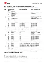
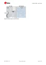
C030-R412M Arduino™ compatible interface details are given in 

Table 6

 and shown in 

Figure 7

. 

Conn.  Pin 

N° 

Arduino 
naming 

Description 

HostMCU port assignment  

Alternate functions and notes 

Ard1

A


n.c. 

Not connected 


IOREF  IO reference voltage level. 

Connected to 3.3 VDC 


Could be used as input for external 
IO level setting.  

nR 

Reset signal input. 
Negative logic 


3.3V 

3.3 VDC supply output  


Controlled by HostMCU Port PE_0 
0: disable, 1:enable 

5V 

5 VDC Reference input 


Could be used as IO Reference input 

GND 

Ground level 


GND 

Ground level 


VIN 

External DC supply input   In the range of 2.5 VDC to 5.5 VDC 

See Jumper J1 in sectio

2.4


Ard1

B


A0 

Analog input 

PA_3 Analog input

6


GPIO, Ext. interrupt 

10 

A1 

Analog input 

PC_0 Analog input

6


GPIO, Ext. interrupt 

11 

A2 

Analog input 

PC_3 Analog input

6


GPIO, Ext. interrupt 

12 

A3 

Analog input 

PA_4 Analog input

6


GPIO, Ext. interrupt 

13 

A4 

Analog input 

PA_6 Analog input

6

, PB_7 I2C1 SDA

7


GPIO, Ext. interrupt 

14 

A5 

Analog input 

PB_0 Analog input

6

, PB_6 I2C1 SCL

8


GPIO, Ext. interrupt 

Ard1C


15 

D0 

Digital I/O, UART RX 

PD_9, USART3_TX 

GPIO, Ext. interrupt 

16 

D1 

Digital I/O, UART TX 

PD_8, USART3_RX 

GPIO, Ext. interrupt 

17 

D2 

Digital I/O 

PD_11 

USART3_CTS, GPIO, External 
interrupt 

18 

D3 

Digital I/O 

PB_14 

USART3_RTS, GPIO, PWM, Ext. 
interrupt 

19 

D4 

Digital I/O 

PC_8 

GPIO, PWM, Ext. interrupt 

20  D5 

Digital I/O 

PA_5 

GPIO, PWM, Ext. interrupt 

21 

D6 

Digital I/O 

PB_8 

GPIO, PWM, Ext. interrupt 

22  D7 

Digital I/O 

PB_15 

GPIO, PWM, Ext. interrupt 

Ard1D


23  D8 

Digital I/O 

PD_15 

GPIO, Ext. interrupt 

24  D9 

Digital I/O 

PD_12 

GPIO, Ext. interrupt 

25  D10

9


Digital I/O 

PE_11, SPI4 NSS, shared with SD Card  GPIO, PWM, Ext. interrupt 

26  D11 

Digital I/O 

PE_6, SPI4 MOSI, shared with SD Card  GPIO, PWM, Ext. interrupt 

27  D12 

Digital I/O 

PE_5, SPI4 MISO, shared with SD Card  GPIO, PWM, Ext. interrupt 

28  D13 

Digital I/O 

PE_2, SPI4 SCK, shared with SD Card 

GPIO, Ext. interrupt 

29  GND 

Ground level 


30  AREF 

3.3 VDC reference 


31 

SDA 

I2C SDA I/O 

PB_6 I2C1 SCL 

GPIO, Ext. interrupt 

32  SCL 

I2C SCL Output 

PB_7 I2C1 SDA 

GPIO, Ext. interrupt 

Table 6: C030-R412M Arduino UNO R3 compatible interface 


6

 Pin is connected to the port via 1 k

Ω

/1 k

Ω

 resistive voltage divider. 

7

 PB_7 could be connected to the (A4) Ard1B pin 13 to provide I2C1 SDA signal. 

8

 PB_6 could be connected to the (A5) Ard1B pin 14 to provide I2C1 SCL signal. 

9

 Arduino interface D10 to D13 pins are used as an SPI Bus to HostMCU SPI4 peripheral. The D10 to D13 pins are shared with the 

SD card socket. 

Содержание C030-R412M

Страница 1: ...ed Enabled IoT starter kit User Guide Abstract This guide explains how to set up the C030 Arm Mbed Enabled Internet of Things Starter Kit to begin evaluating u blox LTE Cat M1 NB1 cellular and GNSS modules www u blox com UBX 19010121 R01 ...

Страница 2: ...number Firmware version PCN reference Product status C030 C030 R412M 0 00 G0 V 00 00 10R UBX 19027009 Initial production u blox or third parties may hold intellectual property rights in the products names logos and designs included in this document Copying reproduction modification or disclosure to third parties of this document or any part thereof is only permitted with the express written permis...

Страница 3: ...nfiguration links components 14 2 6 Test break out points and debug interfaces 18 2 7 Arduino UNO R3 compatible interface pin out 19 2 8 Power supply options and LiPo battery usage 20 3 Getting started 22 3 1 C030 R412M board setup 22 3 2 Development PC USB driver configuration 22 3 3 Getting started with Mbed 22 4 Approvals 23 4 1 European Conformance 23 4 2 US Federal Communications Commission n...

Страница 4: ...for the period of 90 days which can be topped up and extended on demand The u blox C030 R412M board is powered by an Arm Cortex M4 based ST STM32F437VGT Host microcontroller which is fully supported by the Arm Mbed platform The microcontroller has 512 kB flash 64 kB RAM and runs an up to 96 MHz system clock The board provides simple USB drag n drop programming and an ST Link debug interface for th...

Страница 5: ... Replace the battery if it no longer has sufficient charge for unit operation Control the battery before using it if the device has not been operated for an extended period of time C030 R412M application boards comply with the Directive 2011 65 EU of the European Parliament and the Council on the Restriction of Use of certain Hazardous Substances in Electrical and Electronic Equipment EU RoHS 2 an...

Страница 6: ...attery is not included On board SiLabs CP2105 USB to Dual UART Bridge as Serial USB sniffer o Alternative to ST Link V2 1 Virtual COM Port when ST LINK V2 1 is not used available o Alternative to Main Supply and Debug USB 5V VBUS inputs o Sniffing serial communication between the Host MCU and the Cellular module RGB User LED and two push buttons User and Reset On board SiLabs Si7034 A10 Humidity a...

Страница 7: ...C030 R412M User Guide UBX 19010121 R01 Hardware description Page 7 of 27 Figure 1 C030 R412M application board overview ...

Страница 8: ...ze and power consumption The utility section is powered up from the Debug USB 5V VBus When the Debug USB is not connected SW debugging virtual COM port and Ethernet Interface functions are turned off and isolated from the application section The Auxiliary 5V USB connector on the utility section could be used to boost the power input to the application section if the current input from the Debug US...

Страница 9: ...o Uno R3 interface on the application section could be used to integrate sensors actuators and power battery supply circuitries as Arduino Shields expansion daughter PCBs The application section could run standalone when the utility section is snapped off Antenna section The C030 R412M has SMA Jack edge connectors for Cellular and GNSS antennas The C030 R412M major component layout is provided in ...

Страница 10: ...O Port PC13 Application RST1 Reset button Push button to reset the HostMCU Application P1 System power jumper System power input selection Pin 1 2 on board Power Battery Management default configuration Pin 2 3 VIN pin of Arduino Uno R3 interface Application S2 Serial USB sniffer source select Select the cellular module communication UART channel to sniff Position 1 isolation Position 2 UART1 comm...

Страница 11: ...ostMCU USART2 Rx can be connected to cellular modem USB sniffer Standard COM port Tx channel via R137 link see Table 4 In this case do one of the following The utility section should be powered off disconnect Debug USB Snap off the utility section Remove R133 link see Table 4 Enhanced COM port as on the development PC Two operation modes can be selected by using S2 switch see Figure 4 o S2 positio...

Страница 12: ... USB VBUS VBUS 5 V indicator for 5 VDC supply input LED4 Cellular module USB VBUS VBUS 5 V indicator LED5 Battery charging man Input Battery Charging Management 5 VDC input supply indicator LED6 STLink CMSIS DAP status InterfaceMCU Debugging Flashing status RED GREEN indicator LED7 Battery charging status Battery Charging Management battery charging status indicator D3 User RGB LED HostMCU GPIO dr...

Страница 13: ...nterfaceMCU debug Tag Connect NL Plug of Nails connector compatible PCB touch points footprint for InterfaceMCU Utility SWD_TARGET HostMCU debug 10 pin Arm Cortex debug connector for InterfaceMCU may not be populated Application SWD_TGT1 HostMCU debug Tag Connect NL Plug of Nails connector compatible PCB touch points footprint for HostMCU Application ANT Cellular main antenna SMA connector for the...

Страница 14: ...visional4 Link to HostMCU I2C3 SCL bus through 3 3 V to 1 8 V level translator R31 Arduino Interface IOREF to 3 3V 33 Ω link to 3 3 VDC R33 Arduino Interface 3 3V supply Link to 3 3VDC rail R38 Arduino Interface A4 pin voltage divisor 1 kΩ voltage divisor resistor for analog input It could be removed for I2C SDA alternative usage R39 Arduino Interface A5 pin voltage divisor 1 kΩ voltage divisor re...

Страница 15: ...ar module GPIO2 link Link to the HostMCU PD_1 port R103 Cellular module GPIO4 link Not functional R104 Cellular module USB Data_N signal link Cellular module USB signal to J7 cellular module USB connector R105 HostMCU USART1 Tx link When removed isolates HostMCU USART1 Tx pin PA_9 from the cellular module Could be used in a configuration to drive the cellular module from the serial USB sniffer dir...

Страница 16: ...0 is a Temperature and Relative Humidity Sensor power link Link to 1 8VDC supply rail See R48 link for utilization R151 Arduino interface 1 8V IO supply option Provisional R152 Arduino interface IOREF voltage level selection for 3 3VDC Link to Arduino interface 3 3V pin R153 Arduino interface IOREF voltage level selection for 5VDC Link to Arduino interface 5V pin R154 Arduino interface 5V pin to U...

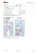
Страница 17: ...face A3 Provisional R184 I_GNSS instrumentation signal link to PB1 Provisional measurement signal R185 USART1_Tx net to PD8 link Link to Arduino interface R186 USART1_Rx net to PD9 link Link to Arduino interface R187 SDCard Detect signal pull up Provisional pull up for PE8 R7122 Arduino interface A0 to MCUWKUP net Provisional Table 4 C030 R412M HW configuration links and components Figure 5 C030 R...

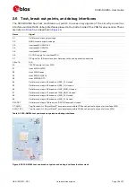
Страница 18: ...8 to 19 N A 20 1 8VDC supply for Host MCU 21 Host MCU SWDIO 22 Host MCU Reset 23 Host MCU SWDCLK 24 Host MCU BOOT0 44 Cellular module pin 44 break out SPK_P Unused 45 Cellular module pin 45 break out SPK_N Unused 46 Cellular module pin 46 break out MIC_BIAS Unused 47 Cellular module pin 47 break out MIC_GND Unused 48 Cellular module pin 48 break out MIC_N Unused 49 Cellular module pin 49 break out...

Страница 19: ... PD_9 USART3_TX GPIO Ext interrupt 16 D1 Digital I O UART TX PD_8 USART3_RX GPIO Ext interrupt 17 D2 Digital I O PD_11 USART3_CTS GPIO External interrupt 18 D3 Digital I O PB_14 USART3_RTS GPIO PWM Ext interrupt 19 D4 Digital I O PC_8 GPIO PWM Ext interrupt 20 D5 Digital I O PA_5 GPIO PWM Ext interrupt 21 D6 Digital I O PB_8 GPIO PWM Ext interrupt 22 D7 Digital I O PB_15 GPIO PWM Ext interrupt Ard...

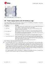
Страница 20: ... 2 3 USB connections are available The LiPo Battery is charged up as well 5 Arduino UNO R3 VIN Pin 8 Arduino UNO R3 VIN pin 8 could be used to power up entire the C030 application section except serial USB sniffer circuitry STLink or CMSIS DAP when available feature could be used through the debug USB However the C030 R412M application section including LiPo Battery management circuitry is disconn...

Страница 21: ...C030 R412M User Guide UBX 19010121 R01 Hardware description Page 21 of 27 Figure 8 C030 power supply connection options ...

Страница 22: ...ecommended to follow the guidelines mentioned below The debug USB port STLink V2 1 interface needs a driver These drivers are available at http www st com content st_com en products embedded software development tool software stsw link009 html Similarly the cellular modem USB sniffer USB port interface needs a driver which is available at http www silabs com products interface usb bridges classic ...

Страница 23: ...for C030 R412M application boards referred to in Article 17 and detailed in Annex III of Directive 2014 53 EU has been followed Thus the following marking is included in the product There are no restrictions for the commercialization of the C030 R412M application boards in all the countries of the European Union Radiofrequency radiation exposure Information this equipment complies with radiation e...

Страница 24: ...12 01 dBi in the 1900 MHz band i e the GSM 1900 LTE FDD 2 band for mobile and fixed or mobile operating configurations 4 3 Innovation Science Economic Development Canada notice ISED Canada formerly known as IC Industry Canada Certification Numbers 8595A UBX18ZO01 Radiofrequency radiation exposure Information this equipment complies with radiation exposure limits prescribed for an uncontrolled envi...

Страница 25: ...imulation System GPIO General Purpose Input Output GSM Global System for Mobile Communication HSPA High Speed Packet Access I2C Inter Integrated Circuit IoT Internet of Things ISED Innovation Science Economic Development LTE Long Term Evolution PCB Printed Circuit Board PWM Pulse Width Modulation RAM Random Access Memory RTS Request To Send SCL Serial Clock SDA Serial Data SIM Subscriber Identific...

Страница 26: ...52 2 u blox SARA R4 SARA N4 series System Integration Manual Doc No UBX 16029218 3 u blox Nested Design Application Note Doc No UBX 16007243 For regular updates to u blox documentation and to receive product change notifications register on our homepage www u blox com Revision history Revision Date Name Comments R01 01 Jul 2019 euyg Initial release ...

Страница 27: ... Office China Beijing Phone 86 10 68 133 545 E mail info_cn u blox com Support support_cn u blox com Regional Office China Chongqing Phone 86 23 6815 1588 E mail info_cn u blox com Support support_cn u blox com Regional Office China Shanghai Phone 86 21 6090 4832 E mail info_cn u blox com Support support_cn u blox com Regional Office China Shenzhen Phone 86 755 8627 1083 E mail info_cn u blox com ...

Отзывы: