Trio CS-1566A Скачать руководство пользователя страница 26

Testing Procedure (refer to Fig. 28): 

1. Connect the output of the square wave 

generator to the input of the amplifier being 

tested. 

2. Connect the  C H 2 probe of the oscilloscope to 

the output of the amplifier being tested. 

3. If the DC component of the circuit being tested 

is sufficiently low to allow both the  A C and DC 

components to be viewed, use the DC position 

of  A C - G N D - D C switch. However, the  A C 

position may be used without affecting the 

results except at very low frequencies, (below 

10 Hz) 

4. Adjust the vertical gain controls for a 

convenient viewing height. 

5. Adjust the sweep time controls for one cycle of 

square wave display on the screen. 

6. For a close-up view of portion of the square 

wave, use the x 10 magnification. 

A n a l y s i n g the  W a v e f o r m s : 

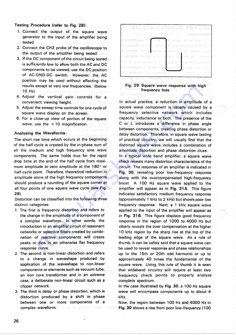
The short rise time which occurs at the beginning 

of the half-cycle is created by the in-phase sum of 

all the medium and high frequency sine wave 

components. The same holds true for the rapid 

drop time at the end of the half cycle from maxi-

mum amplitude to zero amplitude at the  1 8 0 ° or 

half-cycle point. Therefore, theoretical reduction in 

amplitude alone of the high frequency components 

should produce a rounding of the square corner at 

all four points of one square wave cycle (see  F i g . 

29). 

Distortion can be classified into the following three 

distinct categories: 

1. The first is frequency distortion and refers to 

the change in the amplitude of a component of 

a complex waveform. In other words, the 

introduction in an amplifier circuit of reasonant 

networks or selective filters created by combi-

nation of reactive components will create 

peaks or dips in an otherwise flat frequency 

response curve. 

2. The second is non-linear distortion and refers 

to a change in waveshape produced by 

application of the waveshape to non-linear 

components or elements such as vacuum tube, 

an iron core transformer and in an extreme 

case, a deliberate non-linear circuit such as a 

clipper network. 

3. The third is delay or phase distortion, which is 

distortion produced by a shift in phase 

between one or more components of a 

complex waveform. 

In actual practice, a reduction in amplitude of a 

square wave component is usually caused by a 

frequency selective network  w h i c h includes 

capacity, inductance or both. The presence of the 

C or L introduces a difference in phase angle 

between components, creating phase distortion or 

delay distortion. Therefore, in square wave testing 

of practical circuitry,  w e will usually find that the 

distorted square  w a v e includes a combination of 

amplitude distortion and phase distortion clues. 

In a typical wide band amplifier, a square  w a v e 

check reveals many distortion characteristics of the 

circuit. The response of an amplifier is indicated in 

Fig.  3 0 , revealing poor low-frequency response 

along with the overcompensated high-frequency 

boost. A 100 Hz square wave applied to the 

amplifier will appear as in  F i g .  3 1 A. This figure 

indicates satisfactory medium frequency response 

(approximately 1 kHz to 2 kHz) but shows poor low 

frequency response. Next, a 1 kHz square  w a v e 

applied to the input of the amplifier will appear as 

in  F i g .  3 1 B. This figure displays good frequency 

response in the region of  1 0 0 0 to  4 0 0 0 Hz but 

clearly reveals the over compensation at the higher 

10 kHz region by the sharp rise at the top of the 

leading edge of the square wave.  A s a rule of 

thumb, it can be safely said that a square  w a v e can 

be used to reveal response and phase relationships 

up to the 15th or 20th odd harmonic or up to 

approximately  4 0 times the fundamental of the 

square wave. Using this rule of thumb it is seen 

that wideband circuitry will require at least two 

frequency  c h e c k points to properly analyze 

complete spectrum. 

In the case illustrated by  F i g .  3 0 , a  1 0 0 Hz square 

wave will encompass components up to about 4 

kHz. 

Now, the region between  1 0 0 Hz and  4 0 0 0 Hz in 

Fig.  3 0 shows a rise from poor low-frequency  ( 1 0 0 

2 6 

Fig. 29 Square wave response with high 

frequency loss 

Содержание CS-1566A

Страница 1: ...TRIGGERED SWEEP OSCILLOSCOPE HIGH S T A B I L I T Y CS 1566A DUAL TRACE OSCILLOSCOPE INSTRUCTION MANUAL T R I O...

Страница 2: ...observation The time base switch allows changeover between V vertical and H horizontal of VIDEO sync separator circuit automatically and electronically INT C H 1 CH2 LINE and EXT can be individually...

Страница 3: ...time 0 5Ms div to 5s div 5 and X Y 1 2 5 sequence Fine adjustment in all 19 ranges Magnification 10 times 5 PULL x 10 MAG Linearity Better than 3 2 zs div to 0 5s div Better than 5 0 5 s div to 1 s d...

Страница 4: ...tation Trace angle is adjustable by panel surface ad justor Power Requirements Power supply voltage 100 120 220 240V 10 50 60 Hz Power consumption 47W Dimensions Width 260 mm 277 mm Height 190 mm 204...

Страница 5: ...CONTROLS ON PANELS FRONT PANEL Fig 1 REAR PANEL Fig 2 5...

Страница 6: ...Dual trace operation in which sweep is chopped at approximate 200 kHz rate and switched between Channel 1 and Channel 2 traces Recommended for sweep times of 0 5 s div to 1 ms div ADD The waveforms f...

Страница 7: ...tive going sync pulse 19 LEVEL PULL AUTO Sync level adjustment determines points on waveform slope where sweep starts equals most negative point of triggering and equals most positive point of trigger...

Страница 8: ...40V be sure to use a 0 5A fuse 29 POWER CONNECTOR For connection of the supplied AC power cord 30 Z AXIS INPUT Intensity modulation terminal T T L logic compatible high logic increase brightness low l...

Страница 9: ...djust VOLTS DIV 4 7 and VARIABLE 5 8 so that the pulse amplitude is set to the 0 and 100 scales 2 Turn SWEEP TIME DIV 21 to magnify the rising portion of the waveform as large as possible VARIABLE 22...

Страница 10: ...ative going waveform In this case the output waveform is shifted with respect to the leading edge of the Fig 5 Waveforms in divide by two circuit reference frequency pulse by a time interval cor respo...

Страница 11: ...of the waveforms change depending upon the input or more mode of opera tion Ffg 8 shows a typical digital circuit and identifies several of the points at which waveform measure ment are appropriate T...

Страница 12: ...uch cases it is recommended that the sync re main unchanged while the sweep speed or X 1 0 Fig 8 Typical digital circuit using several time related waveforms MAG used be to expaned the waveform displa...

Страница 13: ...e amplifier unit may be measured for distortion with this oscilloscope This type of measurement is especially variable when the slope of a waveform must be faithfully reproduced by an amplifier Fig 10...

Страница 14: ...ns Fig 11 shows a burst circuit The basic settings are identical to those of in Fig 5 Waveform EA is the reference waveform and is applied to CH1 input All other waveforms are sampled at CH2 and compa...

Страница 15: ...Y P E T O H O R I Z O N T A L A M P L I F I E R T O V I D E O O U T P U T A M P L I F I E R N O T E NO E L E C T R I C A L C O N N E C T I O N P L A C E C L I P ON I N S U L A T I O N O F P L A T E C...

Страница 16: ...ut jack The VARIABLE control is adjusted as required to provide a complete cycle of the input waveform displayed on 8 div horizontally A waveform height of 2 div is used The 8 div display represents 3...

Страница 17: ...abled to see the VITS The transmitted VITS is precision sequence of a specific frequences amplitudes and waveshapes as shown in Fig 16 Television networks use the precision signals for adjustment and...

Страница 18: ...s on either side This suggests an IF trap is detuned into the passband chopping out frequencies about 2 MHz below the picture carrier frequency Switch to another channel carrying VITS If the same thin...

Страница 19: ...ection moving the trace to the left until the expanded VITS information appears as shown in Fig 16 Because of the low repetition rate and the high sweep speed combination the brightness level of the s...

Страница 20: ...he peak to peak voltage readings on the oscilloscope with those shown on the waveform pictures Any abnormal readings should be followed by additional readings in the suspected circuits until the troub...

Страница 21: ...controls for the desired brightness and best focus 15 To view a specific portion of the waveform such as the color burst pull outward on the POSITION control for X10 magnification Rotate the same con...

Страница 22: ...tal gain controls for a display similar to that shown in Fig 23A 5 Set the marker generator precisely to 10 7 MHz The marker pip should be in the center of the bandpass 6 Align the IF amplifiers accor...

Страница 23: ...e waveform A sine wave input is applied to the audio circuit being tested The same sine wave input is applied to the vertical input of the oscilloscope and the output of the tested circuit is applied...

Страница 24: ...ces a circular oscilloscope pattern Phase shift of less or more than 90 produces an elliptical oscilloscope pattern The amount of phase shift can be calculated from the oscilloscope trace as shown in...

Страница 25: ...can evaluate the input and output quality of a signal of many frequencies the harmoniques of the square wave which is what the amplifier sees when amplifying complex wave forms of musical instruments...

Страница 26: ...ase a deliberate non linear circuit such as a clipper network 3 The third is delay or phase distortion which is distortion produced by a shift in phase between one or more components of a complex wave...

Страница 27: ...lts are opposite in the two cases because of the difference in polarity of the phase angle in the two cases that can be checked through algebraic addition of components Fig 36 indicates low frequency...

Страница 28: ...the square wave indicates a transient oscillation in a relatively high Q network in the amplifier circuit In this case the sudden transition in the square wave potential from a sharply rising relativ...

Страница 29: ...tuated fundamental C High frequency loss No phase shift D Low frequency phase shift E Low frequency loss and phase shift F High frequency loss and low frequency phase shift G High frequency loss and p...

Страница 30: ...or EXT TRIG is up to 50V DC AC peak and the input to Z AXIS is up to 50V DC AC peak 4 Do not increase the brightness of the CRT unnecessarily 5 Do not leave the oscilloscope for a long period with a b...

Страница 31: ...adjustments use a well insulated screw driver 3 Before marking adjustments be sure to turn on the power and wait until the unit is stabilized 4 For adjustment follow the procedures described below 5...

Страница 32: ...the trace comes to the position of the line in CH2 NOR mode when the CH2 polarity is inverted Horizontal Position Adjustment 1 To adjust the horizontal position under the nor mal sweep condition set t...

Страница 33: ...SCHEMATIC DIAGRAM CS 1566A 33...

Страница 34: ...A p r o d u c t of T R I O K E N W O O D C O R P O R A T I O N 17 5 2 chome Shibuya Shibuya ku Tokyo 150 Japan 2 5 3 1 2 PRINTED IN J A P A N B50 2918 00 G...

Отзывы: