


TMC262-EVAL MANUAL (V. 1.0 / 2011-Sep-07)
6
Copyright © 2010 TRINAMIC Motion Control GmbH & Co. KG
4.1.3
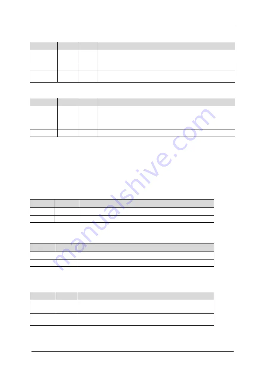
Step and direction input K2
Pin
Number Level
Description
DIR
1
VIO
Direction input of TMC262. Direction output of microcontroller when
enabled via software (step/dir
RUN)
GND
2
GND
Ground reference
STEP
3
VIO
Direction input of TMC262. Step output of microcontroller when
enabled via software (step/dir
RUN)
4.1.4
JTAG programmer K15
Pin
Number Level
Description
NRST
15
3.3V
CPU reset pin. Place a jumper between pin 15 and 16 to disable the
CPU. In this mode, the CPU does not drive the TMC262, and you
can freely access its SPI interface via the header connectors next to
the TMC262.
GND
16
GND
Ground
This connector can be used for debugging of CPU software and for programming via JTAG.
4.1.5
USB (K17) and RS232 (K16)
PC interface for operation with the demonstration software. The USB port is handled as a virtual COM
port.
4.2 Jumpers
4.2.1
Clock selection J1
Setting
Function
Description
1-2
GND
TMC262 uses internal clock
2-3
CLK_ARM TMC262 uses clock signal provided by the microcontroller.
4.2.2
VCC_IO J6
Selects the VCC_IO voltage source for the TMC262.
Setting
Function Description
1-2
3V3
3.3V supply of microcontroller
2-3
5V
5V voltage supplied by TMC262 voltage regulator
4.2.3
VSENSE J8, J11 (J15, J16)
J8 and J11 select the source of the sense resistor voltage of the TMC262. Always use position 1-2 for
normal operation.
Setting
Function Description
1-2
sense
resistor
Normal operation, the TMC262 uses the shunt resistors for current
sensing
2-3
external
input
Sense resistor signals can be supplied via J15 or J16 for testing
purpose


