


TC32306FTG
2015-10-01
49
Notice:
-
To shorten the boot sequence of this IC, there is other way to be able to moving to Run without
going through Standby. In this method, firstly set ENB pin = "H", h'0A [D7] ENB = "1" and h'0A
[D6] ACT = "1", then set other registers. But in this way, if the internal setup and the register
setting are overlapped each other, unexpected operation may occur. To avoid above, make the SPI
speed too fast enough to communicate, or select the previous way as in Fig 6-30.
-
In TX duration DATA_IO pin accepts data input, but that data is not transmitted when status of
PA is Disable. Input data is invalid before PA enabling.
-
Check the relationship between supply voltage and reset, when to utilize the power on reset
during boot sequence. (See the notice in 6.3.1)
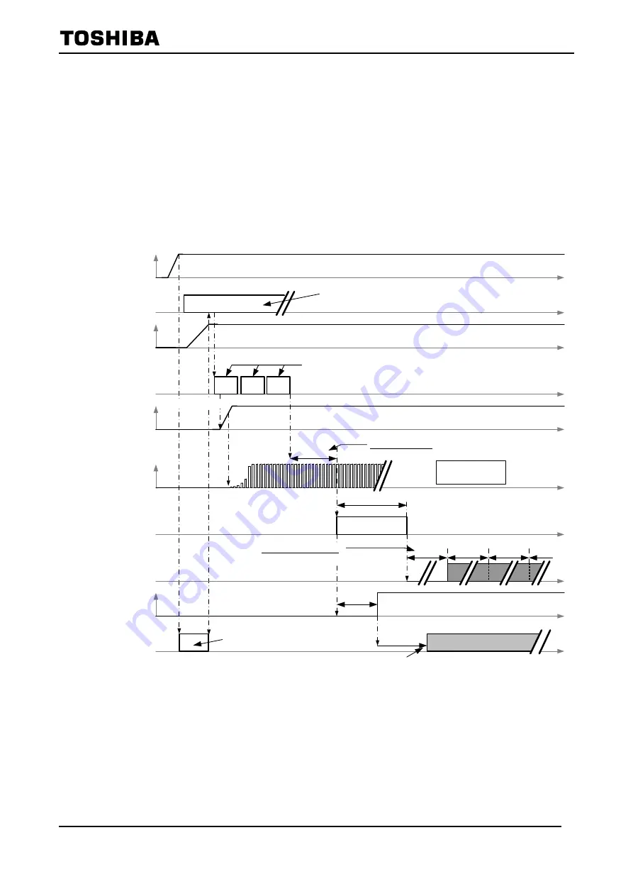
- Example of Boot Sequence 3: RX (in EEPROM Mode)
The following Fig 6-31 shows boot sequence of RX in EEPROM Mode.
Fig 6-31 Example of Boot Sequence Timing Chart (EEPROM Mode / RX)
* The example of timing chart may be omitted or simplified for explanatory purposes.
1.
Power On, and reset is released after the voltage supply becomes stable.
2.
Start to read the register of first set data area of EEPROM sequentially. (It is indicated by the
combination of TX_SW pin, RX_SW pin and ENB pin.)
3.
Start to operate with Standby despite of the value of the register:h’0A[D6]ACT. Internal
regulators and Reference Clock Oscillator start to operate.
4.
Read the second and third set data area continuously then the register setting is fixed.
5.
Continue to operate depending on the setting of the register:h’0A[D6]ACT.
EEPROM Data
Internal Regulator
(voltage)
Level of
Reference Clock
Internal Counter
Demodulation Output
: at DATA_IO pin
RESET
Voltage Supply
PLL_LD Signal
: at DET_TMONI1 / 2 pin
Signal Detections
(RSSI / Noise Detection)
: at DET_TMONI1 / 2 pin
Pins to set
the Configuration
(RX_SW/TX_SW/ENB)
About
0.1ms
Detection Cycle Setting
* 0.338ms / 0.675ms / 1.35ms / 2.70ms
1.35ms
1.35ms
1.35ms
1.35ms
About 0.22ms
Internal Setup
105.5µs
*: Initial Value
It indicates typical.
Delay Time Setting
* 105.5
μ
s / 211.1
μ
s / 316.5
μ
s / 527.5
μ
s / 949.5
μ
s
Start with Standby
1st
Start to read EEPROM
(Read the data three times as majority logic)
2nd
3rd
Pointing the Configuration
The configuration is selected by the combination of
TX_SW/RX_SW/ENB pin status when reset is released.
(For example, RX_SW=High / TX_SW=Low / ENB=High)
Start of the demodulation output depends on Bit Rate
Filter setting or others.
High Impedance
Demodulation
Output