Specification No. TENTATIVE
Sheet
23
Toshiba Matsushita Display Technology Co.,Ltd
Date: 2008 – 11- 07
Date: - -
New No. LTA057A341F-14
Old No.
←
# Special
←&
Addition
←
Change
3. Recommended Operating Conditions
1)
Item Symbol
Min.
Typ.
Max.
Unit
Remarks
Supply Voltage
2)
V
DD
3.0 3.3 3.6
V
Forward current
4)
I
LED
--- 15.0 25.0 mA
Forward voltage
4)
V
LED
18.0 19.2 19.8 V
"H" Level input
3)
V
IH
0.8V
DD
---
V
DD
V
"L" Level Input
3)
V
IL
0 ---
0.2
V
DD
V
Note 1) The module should be always operated within these ranges. The "Typ." shows the recommendable value.
Note 2) Checked Pin Terminal:
V
DD
(GND:
V
SS
=0V)
Note 3) Checked Pin Terminal: R5 to R0, G5 to G0, B5 to B0, CLK, DE, H-sync, V-sync (GND:
V
SS
=0V)
Note 4) One row LEDs (six-piece series connection) at 25 degrees C.
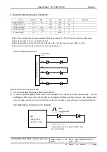
LED back light equivalent circuit
Note) Cautions on use the circuit of LED
1) The current feedback function is needed to each LED line.
2) To control brightness applying PWM (Pulse Width Modulation) drive should be strongly recommended. If to dim
brightness by LED current control, LED white color chromaticity distribution will become large. And applying same
wave form (peak, width & duty) for each LED lines is also recommended to prevent enlarge chromaticity distribution.
RECOMMENDED LED DRIVING BLOCK DIAGRAM
LED
driving circuit
(Customer side)
PWM
current output
Keep same wave form (peak, width & duty)
for each LED lines.
Connector (
C
N2)
Terminal No.
No.1
No.3
No.4
No.5
No.6
No.2


