


Specification No. TENTATIVE
Sheet
27
Toshiba Matsushita Display Technology Co.,Ltd
Date: 2008 – 11- 07
Date: - -
New No. LTA057A341F-14
Old No.
←
# Special
←&
Addition
←
Change
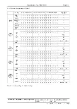
6.4 Appearance Test
6.4.1 Test Conditions
1) Condition : Non-operating, operating
Same as 4.1 and 6.2
6.4.2 Specifications
Item Description
Class
Pattern peeling snapping, electrically short
PCB Appearance
Repair portion on PCB is not covered by epoxy resign
Major
Soldering
Cold solder joint, lead move when pulled
Minor
Bezel, Frame,
Connectors
Distinct stain, rust or scratch which relate with LCD display performance and
reliability
Major
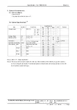
Line width
Length(mm)
Acceptable count
W
≤
0.05
neglect
0.05
<
W
≤
0.07
n
≤
8
0.07
<
W
≤
0.10
n
≤
2
0.10
<
W
L
≤
3
2)
Average diameter(mm)
Acceptable count/side
D
≤
0.2
neglect
0.2
<
D
≤
0.35
n
≤
5
0.35
<
D
≤
0.5
n
≤
2
0.5
<
D
0
Black and White
Spots/Lines
1)2)3)
Minor
Note 1) Inspection area should be within viewing area.
Note 2) Dusts which are bigger not less than 0.10mm (0.1
≤
W
) shall be judged by "Average Diameter".
Average Diameter
D
= (a+b)/2
Note 3) The dust on the surface which can be removed is not made an issue.
a
b