background image

User’s Manual   

69

PART 3  TC218

5.  I/O Allocation and Programming

5.  I/O Allocation and Programming

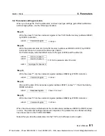
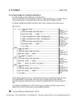
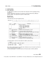
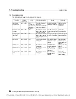
5.1  Allocation to the T2 registers

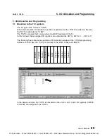
The I/O type of the TC218 is "X 8W".
When the automatic I/O allocation operation is performed with a TC218 mounted on the rack,
the TC218 is allocated as "X 8W".
The TC218 occupies the 8 consecutive input (XW) registers of the T2.
In this manual, these assigned I/O registers are expressed as  XW(n), XW(n+1), ... XW(n+7).

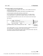
The following figure shows an example of I/O allocation window of the T-PDS programming
software. In this case, the TC218 is mounted in the slot 0 of base unit BU218.

In the above example, the TC218 is allocated on the unit-0, slot-0. And 8 I/O registers, XW000
to XW007 are assigned to the TC218.

PS261

PU

234E

N

o s

lot

DI

3

2

Vac

ant

DO

3

2

T

C

218

Vac

ant

Vac

ant

Vac

ant

Vac

ant

CTi Automation - Phone: 800.894.0412 - Fax: 208.368.0415 - Web: www.ctiautomation.net - Email: [email protected]

Содержание AD268

Страница 1: ...ROGRAMMABLE CONTROLLER PROSEC T2 series ANALOG I O MODULES AD268 DA264 TC218 USER S MANUAL TOSHIBA CORPORATION CTi Automation Phone 800 894 0412 Fax 208 368 0415 Web www ctiautomation net Email info ctiautomation net ...

Страница 2: ...blication Toshiba Corporation reserves the right to make changes and improvements to this publication and or related products at any time without notice No obligation shall be incurred other than as noted in this publication This publication is copyrighted and contains proprietary material No part of this book may be reproduced stored in a retrieval system or transmitted in any form or by any mean...

Страница 3: ...ribed in the T2 T2E or T2N User s Manual before using this module Follow the instructions described in this manual and in the T2 T2E or T2N User s Manual when installing and wiring this module This module has been designed for the T2 T2E T2N Use your AD268 DA264 TC218 only on the T2 series PLC rack These modules consume the internal 5 Vdc power as shown below AD268 300 mA DA264 230 mA TC218 300 mA...

Страница 4: ...nd maintenance of the basic hardware of the programmable controller T2E The functions of the T2E and how to use them and the information necessary for creating user program are also described T2N User s Manual UM TS02N E001 This manual describes the configuration specification installation wiring and maintenance of the basic hardware of the programmable controller T2N The functions of the T2N and ...

Страница 5: ...arameter setting by software 13 4 Wiring 14 4 1 Terminal arrangement 14 4 2 Signal wiring 15 4 3 Wiring precautions 16 5 I O Allocation and Programming 17 5 1 Allocation to the T2 registers 17 5 2 A D conversion data 18 5 3 Programming 23 6 Parameters 24 6 1 Memory map 24 6 2 Parameter setting procedure 30 6 3 Sample program for setting the parameters 31 7 Troubleshooting 32 7 1 RAS information 32...

Страница 6: ...tting by software 40 4 Wiring 41 4 1 Terminal arrangement 41 4 2 Signal wiring 42 4 3 Wiring precautions 43 5 I O Allocation and Programming 44 5 1 Allocation to the T2 registers 44 5 2 D A conversion data 45 5 3 Programming 50 6 Parameters 51 6 1 Memory map 51 6 2 Sample program to access the parameters 55 7 Troubleshooting 56 7 1 RAS information 56 7 2 Troubleshooting 56 CTi Automation Phone 800...

Страница 7: ...are 65 4 Wiring 66 4 1 Terminal arrangement 66 4 2 Signal wiring 67 4 3 Wiring precautions 68 5 I O Allocation and Programming 69 5 1 Allocation to the T2 registers 69 5 2 A D conversion data 70 5 3 Programming 74 6 Parameters 75 6 1 Memory map 75 6 2 Parameter setting procedure 81 6 3 Sample program for setting the parameters 82 7 Troubleshooting 83 7 1 RAS information 83 7 2 Troubleshooting 84 C...

Страница 8: ...6 Analog I O Modules AD268 DA264 TC218 CTi Automation Phone 800 894 0412 Fax 208 368 0415 Web www ctiautomation net Email info ctiautomation net ...

Страница 9: ...D268 1 Introduction 8 2 Specifications 10 3 Input Type Setting 12 4 Wiring 14 5 I O Allocation and Programming 17 6 Parameters 24 7 Troubleshooting 32 CTi Automation Phone 800 894 0412 Fax 208 368 0415 Web www ctiautomation net Email info ctiautomation net ...

Страница 10: ...n process the analog signals 1 1 AD268 Functions The AD268 has the following functions 1 8 channels input per module 2 Selectable input type 5V 10V 0 to 5V 0 to 10V 1 to 5V 0 to 20mA 4 to 20mA 3 16 bit high resolution A D conversion 4 High speed 1ms channel conversion cycle 5 Gain and offset calibration function 6 Input data averaging function 7 Unused channel skip function CTi Automation Phone 80...

Страница 11: ...tus indication LED Analog input terminal External power supply connection terminal Line ground and Frame ground terminal Terminal block fixing screw 2 points Removable terminal block CTi Automation Phone 800 894 0412 Fax 208 368 0415 Web www ctiautomation net Email info ctiautomation net ...

Страница 12: ...C FS 10V Temperature drift 100ppm C or less Conversion cycle Approx 1ms channel Approx 8ms 8 channels Insulation resistance 10MΩ or more Withstand voltage 1500Vac 1 minute between logic and analog circuits 500Vac 1 minute between analog circuit and external 24V 1500Vac 1 minute between analog circuit and FG LG Status indication 1 green LED On when normal Special function Gain and offset calibratio...

Страница 13: ...ternal control circuit through optical isolator Every time when the T2 CPU requests to read the converted data the internal control circuit sends the data to the T2 CPU The AD268 s parameters are stored in the EEPROM Filter Buffer Multiplexer 1 3 2 Jumper Filter Buffer 1 3 2 Jumper A D conversion Optical isolation CH1 P N Internal control circuit CH8 P N Filter DC DC converter Voltage check circui...

Страница 14: ...llocation 5 Program the input type setting program see the next page 6 Turn the T2 to RUN mode 3 1 Jumper plug setting 8 jumper plugs are provided on the AD268 board The jumper plug setting is for selecting either voltage input or current input JP1 is for channel 1 JP2 is for channel 2 JP8 is for channel 8 Jumper plugs JP1 to JP8 1 3 Set the jumper plugs for each channel Side 1 Voltage input Side ...

Страница 15: ...68 Input type parameter data Input type Parameter data Voltage input Current input 0 0 to 5V 0 to 20mA 1 0 to 10V 2 1 to 5V 4 to 20mA 4 5V 5 10V AD268 buffer memory address H8018 Input type for channel 1 H8019 Input type for channel 2 H801A Input type for channel 3 H801B Input type for channel 4 H801C Input type for channel 5 H801D Input type for channel 6 H801E Input type for channel 7 H801F Inpu...

Страница 16: ... Signal name Function 1 1P 2 1N Channel 1 input 3 2P 4 2N Channel 2 input 5 3P 6 3N Channel 3 input 7 4P 8 4N Channel 4 input 9 5P 10 5N Channel 5 input 11 6P 12 6N Channel 6 input 13 7P 14 7N Channel 7 input 15 8P 16 8N Channel 8 input 17 P24 External 24Vdc power 18 COM External 24Vdc power 19 LG Line filter ground 20 FG Frame ground CTi Automation Phone 800 894 0412 Fax 208 368 0415 Web www ctia...

Страница 17: ... AG 15V nP nN Internal circuit Shielded twisted pair cable n Channel number 1 to 8 AG Analog ground FG Frame ground AG 250 Set the jumper plug to Side 3 1 2 3 Current source AD268 P24 COM Internal circuit Normally connect LG and FG then connect to ground a However depending on the condition connect grounding individually by opening LG and FG b AD268 LG FG 24Vdc 10 b a DC DC converter 15V 15V AG CT...

Страница 18: ... same time applying T2 s main power Otherwise this module detects the external 24Vdc error 4 If the external 24Vdc power for this module is not stable the converted data will not be stable In this case use a dedicated 24Vdc power supply for this module 5 It is recommended to short the unused channels Because if it is open for voltage input meaningless A D conversion data will appear 6 If the conve...

Страница 19: ...T2 In this manual these assigned I O registers are expressed as XW n XW n 1 XW n 7 The following figure shows an example of I O allocation window of the T PDS programming software In this case the AD268 is mounted in the slot 0 of base unit BU218 In the above example the AD268 is allocated on the unit 0 slot 0 And 8 I O registers XW000 to XW007 are assigned to the AD268 PS261 PU234E No slot DI32 V...

Страница 20: ...XW n 5 A D conversion data for channel 6 XW n 6 A D conversion data for channel 7 XW n 7 A D conversion data for channel 8 The conversion data stored in the XW register is dependent on the input type as follows 10V range A D conversion data Input voltage Hexadecimal Integer Resolution Upper limit 10 2V H7F80 32640 Full scale positive 10V H7D00 32000 0 3125mV H0001 1 0 0V H0000 0 0 3125mV HFFFF 1 F...

Страница 21: ...0 3125mV H0001 1 0 0V H0000 0 0 3125mV HFFFF 1 Full scale negative 5V HC180 16000 Lower limit 5 12V HC000 16384 0 3125mV bit HC000 16384 0 H3FFF 16383 5V H3E80 16000 5 1196V 5 12V 5V HC180 16000 Digital value 10 2V 10 2V Analog input Upper limit Lower limit D 3200 A D Digital data A Analog signal V CTi Automation Phone 800 894 0412 Fax 208 368 0415 Web www ctiautomation net Email info ctiautomatio...

Страница 22: ...nteger Resolution Upper limit 10 2V H7F80 32640 Full scale positive 10V H7D00 32000 0 3125mV H0001 1 0 0V H0000 0 0 3125mV bit D 3200 A D Digital data A Analog signal V 0 H3FFF 16383 Analog input 5 1196V Digital value 10 2V H7D00 32000 10 2V 10 CTi Automation Phone 800 894 0412 Fax 208 368 0415 Web www ctiautomation net Email info ctiautomation net ...

Страница 23: ...ositive 5V 20mA H3E80 16000 0 3125mV 0 00125mA H0001 1 0 0V 0mA H0000 0 0 3125mV bit 1 25µA bit 0 to 20mA range D 800 A D Digital data A Analog signal mA 0 H3FFF 16383 Analog input 5 1196V 20 479mA Digital value 10 2V H3E80 16000 10 2V Upper limit Lower limit 5V 20mA 0 to 5V range D 3200 A D Digital data A Analog signal V CTi Automation Phone 800 894 0412 Fax 208 368 0415 Web www ctiautomation net...

Страница 24: ...e 5V 20mA H3200 12800 1 0003125V 4 00125mA H0001 1 Lower limit 1V 4mA H0000 0 0 3125mV bit 1 25µA bit 4 to 20mA range D 800 A 3200 D Digital data A Analog signal mA 1 to 5V range D 3200 A 3200 D Digital data A Analog signal V 0 Analog input value 5 1196V 20 479mA Digital value 10 2V 10 2V Upper limit Lower limit 5V 20mA H3200 12800 H337F 13183 1V 4mA CTi Automation Phone 800 894 0412 Fax 208 368 0...

Страница 25: ...sion data XW005 Channel 6 A D conversion data XW006 Channel 7 A D conversion data XW007 Channel 8 A D conversion data Therefore in the user program you can use these XW registers directly for the analog data processing The program shown below is an example of simple comparison with the channel 1 analog data 10V setting Line 1 When XW000 is greater than 25600 channel 1 analog input is more than 8V ...

Страница 26: ... Offset calibration value for channel 4 H800C Offset calibration value for channel 5 H800D Offset calibration value for channel 6 H800E Offset calibration value for channel 7 H800F Offset calibration value for channel 8 H8010 Averaging times for channel 1 H8011 Averaging times for channel 2 H8012 Averaging times for channel 3 H8013 Averaging times for channel 4 H8014 Averaging times for channel 5 ...

Страница 27: ...hannel 6 H802E Analog input actual value for channel 7 H802F Analog input actual value for channel 8 H8030 Module status for channel 1 H8031 Module status for channel 2 H8032 Module status for channel 3 H8033 Module status for channel 4 H8034 Module status for channel 5 H8035 Module status for channel 6 H8036 Module status for channel 7 H8037 Module status for channel 8 Use READ instruction to rea...

Страница 28: ...d value O Offset calibration value buffer memory address H8008 to H800F G Gain calibration value buffer memory address H8000 to H8007 FS Full scale value 32000 for 10V and 0 to 10V ranges 16000 for 5V 0 to 5V and 0 to 20mA ranges 12800 for 1 to 5V and 4 to 20mA ranges The data setting range of the gain and offset calibration value are as follows Input type Gain calibration value Upper limit 32000 ...

Страница 29: ... range is as follows Input type Averaging times Upper limit 127 Default value 1 All types Lower limit 1 Input type setting H8018 to H801F This parameter is used to select the input type This parameter also has a function to skip the A D conversion for unused channels By using the channel skip function the conversion cycle time can be reduced The available setting range is as follows Input type Set...

Страница 30: ...rror is caused by hardware or external condition the reset command may not be effective The command register and the response register are used for hand shaking Refer to section 6 2 for the parameter setting procedure Response register H8021 This register shows the AD268 s response for the command issued Check the status of this register using READ instruction Value Response Description 0 The requ...

Страница 31: ...hen the channel skip is designated 7 Input type setting error 1 when the input type designation is invalid 8 Wire break 1 when wire breakage is detected Effective only for 4 to 20mA input 9 Input limit 1 when the A D conversion data is limited because of the range over A MPU error 1 when the AD268 s processor is not normal B ROM status 1 when the AD268 s EEPROM is not normal C DP RAM status 1 when...

Страница 32: ... H801F Input type for channel 8 Write the parameter data 32 words Step 3 Write the value 1 into the command register address H8020 by WRITE instruction H8020 Command register Write 1 Step 4 Wait until the data of the response register address H8021 comes 1 Check the data by READ instruction H8021 Response register Check if it comes 1 Step 5 Write the value 0 into the command register address H8020...

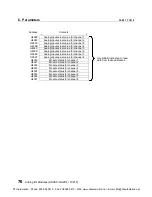
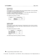
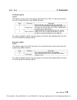
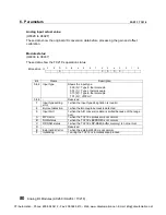
Страница 33: ... set to 0 to 10V for all 8 channels When the parameter setting process is completed the flags R1000 to R1002 are returned to OFF For reading the parameters from the AD268 there is no special procedure Simply read the data from the AD268 s buffer memory by using READ instruction Step 1 Writes 0 into the command register H8020 Step 2 Writes parameters Gain 32000 Offset 0 Average 1 Type 1 0 10V Total...

Страница 34: ... error 1 when the input type designation is invalid 8 Wire break 1 when wire breakage is detected Effective only for 4 to 20mA input 9 Input limit 1 when the A D conversion data is limited because of the range over A MPU error 1 when the AD268 s processor is not normal B ROM status 1 when the AD268 s EEPROM is not normal C DP RAM status 1 when the AD268 s DP RAM buffer memory is not normal D Reser...

Страница 35: ...signal limit over Bit 9 is ON ON The A D conversion data of the channel is limited by the limit value Analog input signal is out of the range Check the signal source sensor MPU error Bit A is ON OFF The A D conversion is stopped Internal processor operation is not normal Execute reset command or cycle power off and on ROM error Bit B is ON OFF The A D conversion is stopped EEPROM data error is det...

Страница 36: ...34 Analog I O Modules AD268 DA264 TC218 CTi Automation Phone 800 894 0412 Fax 208 368 0415 Web www ctiautomation net Email info ctiautomation net ...

Страница 37: ...A264 1 Introduction 36 2 Specifications 38 3 Output Type Setting 40 4 Wiring 41 5 I O Allocation and Programming 44 6 Parameters 51 7 Troubleshooting 56 CTi Automation Phone 800 894 0412 Fax 208 368 0415 Web www ctiautomation net Email info ctiautomation net ...

Страница 38: ...analog signals voltage or current 1 1 DA264 Functions The DA264 has the following functions 1 4 channels output per module 2 Selectable output type 5V 10V 0 to 5V 0 to 10V 1 to 5V 0 to 20mA 4 to 20mA 3 16 bit high resolution D A conversion 4 High speed 1ms channel conversion cycle 5 Offset calibration function 6 Output hold function CTi Automation Phone 800 894 0412 Fax 208 368 0415 Web www ctiaut...

Страница 39: ...tus indication LED Analog output terminal External power supply connection terminal Line ground and Frame ground terminal Terminal block fixing screw 2 points Removable terminal block CTi Automation Phone 800 894 0412 Fax 208 368 0415 Web www ctiautomation net Email info ctiautomation net ...

Страница 40: ...0 2 FS at 25 C 0 5 FS 0 to 55 C FS 10V Temperature drift 100ppm C or less Conversion cycle Approx 1ms channel Approx 4ms 4 channels Insulation resistance 10MΩ or more Withstand voltage 1500Vac 1 minute between logic and analog circuits 500Vac 1 minute between analog circuit and external 24V 1500Vac 1 minute between analog circuit and FG LG Status indication 1 green LED On when normal Special funct...

Страница 41: ...e output to each channel CH1 to CH4 via amplifier Each channel has both the voltage output and the current output However either voltage or current output can be used Internal control circuit LED T2 CPU Optical isolation D A conversion Amplifier Buffer CH1 P N Voltage check circuit 5V 15V 15V AG P24 COM LG FG DC DC converter Filter Regulator Amplifier P N TR V V V I Amplifier Buffer Amplifier TR V...

Страница 42: ...specified by writing the following parameter data into the DA264 s buffer memory To write the parameter into the buffer memory T2 user program WRITE instruction is used These parameter data are not maintained in the DA264 Therefore program the output type setting routine and execute it at each time of the beginning of the operation Output type parameter data Output type Parameter data Voltage outp...

Страница 43: ...tage output 3 1CP 4 1CN Channel 1 Current output 5 2VP 6 2VN Channel 2 Voltage output 7 2CP 8 2CN Channel 2 Current output 9 3VP 10 3VN Channel 3 Voltage output 11 3CP 12 3CN Channel 3 Current output 13 4VP 14 4VN Channel 4 Voltage output 15 4CP 16 4CN Channel 4 Current output 17 P24 External 24Vdc power 18 COM External 24Vdc power 19 LG Line filter ground 20 FG Frame ground CTi Automation Phone 8...

Страница 44: ...DA264 AG 15V 15V nCP nCN Internal circuit Shielded twisted pair cable n Channel number 1 to 4 AG Analog ground DA264 15V DA264 P24 COM LG FG DC DC converter 24Vdc 10 Internal circuit b a Normally connect LG and FG then connect to ground a However depending on the condition connect grounding individually by opening LG and FG b 15V 15V AG CTi Automation Phone 800 894 0412 Fax 208 368 0415 Web www ct...

Страница 45: ...uires 24Vdc power Apply the 24Vdc power before or at the same time applying T2 s main power Otherwise this module detects the external 24Vdc error 4 If the external 24Vdc power for this module is not stable the converted data will not be stable In this case use a dedicated 24Vdc power supply for this module 5 When the external 24Vdc power is applied about 0 7V voltage will output for few ms millis...

Страница 46: ...of the T2 In this manual these assigned I O registers are expressed as YW n YW n 1 YW n 2 and YW n 3 The following figure shows an example of I O allocation window of the T PDS programming software In this case the DA264 is mounted in the slot 0 of base unit BU218 In the above example the DA264 is allocated on the unit 0 slot 0 And 4 I O registers YW000 to YW003 are assigned to the DA264 PS261 PU2...

Страница 47: ...for channel 2 YW n 2 D A conversion data for channel 3 YW n 3 D A conversion data for channel 4 The conversion data to be written into the YW register is dependent on the output type as follows 10V range D A conversion data Hexadecimal Integer Output voltage Resolution Upper limit H7F80 32640 10 2V Full scale positive H7D00 32000 10V H0001 1 0 3125mV 0 H0000 0 0V HFFFF 1 0 3125mV Full scale negati...

Страница 48: ...V H0001 1 0 3125mV 0 H0000 0 0V HFFFF 1 0 3125mV Full scale negative HC180 16000 5V Lower limit HC000 16384 5 12V 0 3125mV bit A 0 3125 D D Digital data A Analog signal mV 5V Analog output value 0 H3FFF 16383 5 1196V 5 12V HC000 16384 5V H7FFF 32767 HC180 16000 H8000 32768 Digital data H3E80 16000 Upper limit Lower limit CTi Automation Phone 800 894 0412 Fax 208 368 0415 Web www ctiautomation net ...

Страница 49: ...Upper limit H7F80 32640 10 2V Full scale positive H7D00 32000 10V H0001 1 0 3125mV 0 H0000 0 0V 0 3125mV bit A 0 3125 D D Digital data A Analog signal mV H8000 32768 0 H7FFF 32767 Analog output value 10V H7D00 32000 Digital data Lower limit CTi Automation Phone 800 894 0412 Fax 208 368 0415 Web www ctiautomation net Email info ctiautomation net ...

Страница 50: ...positive H3E80 16000 5V 20mA H0001 1 0 3125mV 0 00125mA 0 H0000 0 0V 0mA 0 3125mV bit 1 25µA bit 0 to 20mA range A 1 25 D D Digital data A Analog signal µA 0 to 5V range A 0 3125 D D Digital data A Analog signal mV Analog output value 0 H3FFF 16383 Upper limit 5V 20mA H7FFF 32767 H8000 32768 5 1196V 20 478mA H3E80 16000 Digital data Lower limit CTi Automation Phone 800 894 0412 Fax 208 368 0415 We...

Страница 51: ...3125V 4 00125mA 0 H0000 0 1V 4mA Lower limit HF380 3200 0V 0mA 0 3125mV bit 1 25µA bit 4 to 20mA range A 1 25 D 4000 D Digital data A Analog signal µA 1 to 5V range A 0 3125 D 1000 D Digital data A Analog signal mV H8000 32768 0 H7FFF 32767 Analog output value H3200 12800 Digital data 5V 20mA 1V 4mA HF380 3200 H337F 13183 5 1196V 20 478mA Lower limit Upper limit CTi Automation Phone 800 894 0412 F...

Страница 52: ...nnel 2 D A conversion data YW002 Channel 3 D A conversion data YW003 Channel 4 D A conversion data Therefore in the user program you can use any instructions to write data in these YW registers for the analog data processing The program shown below is an example of simple increasing decreasing of the channel 1 analog data 10V setting Rung 1 During R1000 is ON YW000 data is increased by 32 channel ...

Страница 53: ...alue for channel 2 H8002 Offset calibration value for channel 3 H8003 Offset calibration value for channel 4 H8004 Output type setting for channel 1 H8005 Output type setting for channel 2 H8006 Output type setting for channel 3 H8007 Output type setting for channel 4 H8008 Analog output read back value for channel 1 H8009 Analog output read back value for channel 2 H800A Analog output read back v...

Страница 54: ...sion is performed as follows When the offset calibration value is set this value is added to the original D A conversion data Then D A conversion is performed in the DA264 The data setting range of the offset calibration value are as follows Output calibration range Offset calibration value Voltage Current Upper limit 127 39 69 mV 158 75 µA Default value 0 0 0 Lower limit 127 39 69 mV 158 75 µA An...

Страница 55: ...peration when the controller T2 is operating normally However when the T2 stops the operation by Halt mode or Error mode the DA264 s output status is different between these modes Refer to the table below Mode Condition Output type Analog output status T2 is in normal operation Any Normal output 1 to 5V 4 to 20mA 1V 4mA T2 is in Halt or Error mode Other than above 0V 0mA T2 s main power is off Any...

Страница 56: ...e output type 000 0 0 to 5V 0 to 20mA 001 1 0 to 10V 010 2 1 to 5V 4 to 20mA 100 4 5V 101 5 10V 3 to 4 Reserved 5 to 7 Hold mode Shows the output mode clear mode normal or hold mode 101 Hold mode Other than above Clear mode 8 Output type setting error 1 when the output type designation is invalid 9 to C Reserved D Output limit 1 when the D A conversion data is limited because of the range over E E...

Страница 57: ...that he DA264 is allocated to YW000 to YW003 For details of READ and WRITE instructions refer to the T series Instruction Set manual Main program In this sample program the rung 1 is activated at the beginning of RUN mode at the second scan automatically The output type is set to 10V for all 4 channels The rung 2 is to read the analog output read back values and the module status These data are re...

Страница 58: ...odule operation Cause Remedy Output type setting error Bit 8 is ON ON if the error occurs in all channels it is OFF The D A conversion continues based on the previous setting Invalid output type parameter was set Set the correct output type parameter D A conversion data limit over Bit D is ON ON The D A conversion data of the channel is limited by the limit value The written D A conversion data is...

Страница 59: ...User s Manual 57 CTi Automation Phone 800 894 0412 Fax 208 368 0415 Web www ctiautomation net Email info ctiautomation net ...

Страница 60: ...58 Analog I O Modules AD268 DA264 TC218 CTi Automation Phone 800 894 0412 Fax 208 368 0415 Web www ctiautomation net Email info ctiautomation net ...

Страница 61: ...e TC218 1 Introduction 60 2 Specifications 62 3 Input Type Setting 64 4 Wiring 66 5 I O Allocation and Programming 69 6 Parameters 75 7 Troubleshooting 83 CTi Automation Phone 800 894 0412 Fax 208 368 0415 Web www ctiautomation net Email info ctiautomation net ...

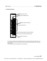
Страница 62: ...tor is attached with the TC218 On the other hand when the TC218 is used for 100mV input it has 8 channels of input 1 1 TC218 Functions The TC218 has the following functions 1 7 channels input per module for thermocouple input 8 channels input per module for 100mV input 2 Selectable input type Thermocouple type K 200 to 1200 C Thermocouple type J 200 to 800 C Thermocouple type E 200 to 600 C 100mV ...

Страница 63: ...mbient temperature for cold junction compensation For 100mV input all 8 channels CH1 to CH8 are used Model type TC218 Status indication LED Analog input terminal External power supply connection terminal Line ground and Frame ground terminal Terminal block fixing screw 2 points Removable terminal block CTi Automation Phone 800 894 0412 Fax 208 368 0415 Web www ctiautomation net Email info ctiautom...

Страница 64: ...0ppm C or less Conversion cycle Approx 1ms channel Approx 8ms 8 channels Insulation resistance 10MΩ or more Withstand voltage 1500Vac 1 minute between logic and analog circuits 500Vac 1 minute between analog circuit and external 24V 1500Vac 1 minute between analog circuit and FG LG Status indication 1 green LED On when normal Special function Gain and offset calibration function mV input only Line...

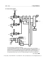
Страница 65: ...optical isolator Every time when the T2 CPU requests to read the converted data the internal control circuit sends the data to the T2 CPU The TC218 s parameters are stored in the EEPROM Filter Buffer 1 3 2 Jumper Filter Buffer 1 3 2 Jumper A D conversion Optical isolation CH1 P N Internal control circuit CH8 P N Filter DC DC converter Voltage check circuit Regulator 5V 15V 15V AG P24 COM LG FG EEP...

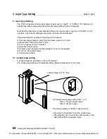
Страница 66: ...Mount the TC218 onto the T2 rack 3 Turn on power to the T2 system 4 Execute I O allocation 5 Program the input type setting program see the next page 6 Turn the T2 to RUN mode 7 Cycle power off on 3 1 Jumper plug setting 8 jumper plugs are provided on the TC218 board The jumper plug setting is for selecting either thermocouple input or mV input Jumper plugs JP1 to JP8 1 3 Set all the jumper plugs ...

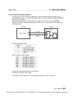
Страница 67: ...ameter data Parameter data Input type 0 Type K thermocouple 1 Type J thermocouple 2 Type E thermocouple 5 100mV TC218 buffer memory address H8018 Input type for channel 1 H8019 Input type for channel 2 H801A Input type for channel 3 H801B Input type for channel 4 H801C Input type for channel 5 H801D Input type for channel 6 H801E Input type for channel 7 H801F Input type for channel 8 Set the same...

Страница 68: ... Signal name Function 1 1P 2 1N Channel 1 input 3 2P 4 2N Channel 2 input 5 3P 6 3N Channel 3 input 7 4P 8 4N Channel 4 input 9 5P 10 5N Channel 5 input 11 6P 12 6N Channel 6 input 13 7P 14 7N Channel 7 input 15 8P 16 8N Channel 8 input 17 P24 External 24Vdc power 18 COM External 24Vdc power 19 LG Line filter ground 20 FG Frame ground CTi Automation Phone 800 894 0412 Fax 208 368 0415 Web www ctia...

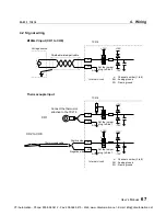
Страница 69: ...round FG Frame ground V 1 2 3 Voltage source TC218 15V 15V AG 15V 1P 1N 1 2 3 TC218 Set the jumper plug to Side 1 15V AG 15V nP nN Internal circuit n Channel number 2 to 8 AG Analog ground FG Frame ground 1 2 3 Set the jumper plug to Side 1 15V Thermocouple cable Positive side Negative side Connect the thermistor attached to the TC218 CTi Automation Phone 800 894 0412 Fax 208 368 0415 Web www ctia...

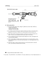
Страница 70: ...ly for this module 4 It is recommended to short the unused channels Because if it is open meaningless A D conversion data will appear 5 If the converted data is not stable owing to electrical noise it is recommended to use the input averaging function to reduce the noise interference For the averaging function refer to section 6 6 When this module is used for thermocouple input connect the thermis...

Страница 71: ...T2 In this manual these assigned I O registers are expressed as XW n XW n 1 XW n 7 The following figure shows an example of I O allocation window of the T PDS programming software In this case the TC218 is mounted in the slot 0 of base unit BU218 In the above example the TC218 is allocated on the unit 0 slot 0 And 8 I O registers XW000 to XW007 are assigned to the TC218 PS261 PU234E No slot DI32 V...

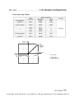
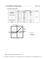
Страница 72: ... 5 A D conversion data for channel 6 XW n 6 A D conversion data for channel 7 XW n 7 A D conversion data for channel 8 The conversion data stored in the XW register is dependent on the input type as follows 100mV input A D conversion data Input voltage Hexadecimal Integer Resolution Upper limit 102mV H7F80 32640 Full scale positive 100mV H7D00 32000 3 125µV H0001 1 0 0V H0000 0 3 125µV HFFFF 1 Ful...

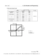
Страница 73: ...0 C H6B08 27400 Full scale positive 1200 C H5DC0 24000 0 05 C H0001 1 0 0V H0000 0 0 05 C HFFFF 1 Full scale negative 200 C HF060 4000 Lower limit 270 C HEAE8 5400 0 05 C bit D 20 A D Digital data A Temperature C 0 Temperature HF060 4000 Digital vale 200 C Upper limit 1200 C H5DC0 24000 Lower limit CTi Automation Phone 800 894 0412 Fax 208 368 0415 Web www ctiautomation net Email info ctiautomatio...

Страница 74: ...er limit 1200 C H5DC0 24000 Full scale positive 800 C H3E80 16000 0 05 C H0001 1 0 0V H0000 0 0 05 C HFFFF 1 Full scale negative 200 C HF060 4000 Lower limit 210 C HEF98 4200 0 05 C bit D 20 A D Digital data A Temperature C 0 Temperature HF060 4000 Digital vale 200 C Upper limit 800 C H3E80 16000 Lower limit CTi Automation Phone 800 894 0412 Fax 208 368 0415 Web www ctiautomation net Email info ct...

Страница 75: ...00 C H4E20 20000 Full scale positive 600 C H2EE0 12000 0 05 C H0001 1 0 0V H0000 0 0 05 C HFFFF 1 Full scale negative 200 C HF060 4000 Lower limit 270 C HEAE8 5400 0 05 C bit D 20 A D Digital data A Temperature C 0 Temperature HF060 4000 Digital vale 200 C Upper limit 600 C H2EE0 12000 Lower limit CTi Automation Phone 800 894 0412 Fax 208 368 0415 Web www ctiautomation net Email info ctiautomation...

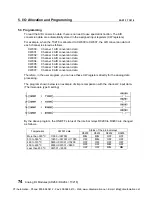
Страница 76: ...ion data XW006 Channel 7 A D conversion data XW007 Channel 8 A D conversion data Therefore in the user program you can use these XW registers directly for the analog data processing The program shown below is an example of simple comparison with the channel 2 input data Thermocouple type K setting By the above program the ON OFF status of the internal relays R0200 to R0203 are changed as follows S...

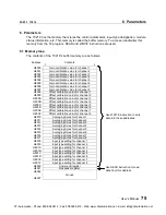
Страница 77: ...ibration value for channel 4 H800C Offset calibration value for channel 5 H800D Offset calibration value for channel 6 H800E Offset calibration value for channel 7 H800F Offset calibration value for channel 8 H8010 Averaging times for channel 1 H8011 Averaging times for channel 2 H8012 Averaging times for channel 3 H8013 Averaging times for channel 4 H8014 Averaging times for channel 5 H8015 Avera...

Страница 78: ...value for channel 6 H802E Analog input actual value for channel 7 H802F Analog input actual value for channel 8 H8030 Module status for channel 1 H8031 Module status for channel 2 H8032 Module status for channel 3 H8033 Module status for channel 4 H8034 Module status for channel 5 H8035 Module status for channel 6 H8036 Module status for channel 7 H8037 Module status for channel 8 Use READ instruc...

Страница 79: ...ffset processed value O Offset calibration value buffer memory address H8008 to H800F G Gain calibration value buffer memory address H8000 to H8007 The data setting range of the gain and offset calibration value are as follows Input type Gain calibration value Upper limit 32000 Default value 32000 100mV Lower limit 10000 Thermocouple Not applicable Input type Offset calibration value Upper limit 3...

Страница 80: ...ilable setting range is as follows Input type Averaging times Upper limit 127 Default value 1 All types Lower limit 1 Input type setting H8018 to H801F This parameter is used to select the input type This parameter also has a function to skip the A D conversion for unused channels By using the channel skip function the conversion cycle time can be reduced The available setting range is as follows ...

Страница 81: ...ed by hardware or external condition the reset command may not be effective The command register and the response register are used for hand shaking Refer to section 6 2 for the parameter setting procedure Response register H8021 This register shows the TC218 s response for the command issued Check the status of this register using READ instruction Value Response Description 0 The requested comman...

Страница 82: ...couple 101 5 100mV 3 to 6 Reserved 7 Input type setting error 1 when the input type designation is invalid 8 Burnout detection 1 when thermocouple burnout is detected 9 Input limit 1 when the A D conversion data is limited because of the range over A MPU error 1 when the TC218 s processor is not normal B ROM status 1 when the TC218 s EEPROM is not normal C DP RAM status 1 when the TC218 s DP RAM b...

Страница 83: ...type for channel 8 Write the parameter data 32 words Step 3 Write the value 1 into the command register address H8020 by WRITE instruction H8020 Command register Write 1 Step 4 Wait until the data of the response register address H8021 comes 1 Check the data by READ instruction H8021 Response register Check if it comes 1 Step 5 Write the value 0 into the command register address H8020 by WRITE ins...

Страница 84: ... type is set to the type J thermocouple for all 8 channels When the parameter setting process is completed the flags R1000 to R1002 are returned to OFF For reading the parameters from the TC218 there is no special procedure Simply read the data from the TC218 s buffer memory by using READ instruction Step 1 Writes 0 into the command register H8020 Step 2 Writes parameters Gain 32000 Offset 0 Avera...

Страница 85: ...t type designation is invalid 8 Burnout detection 1 when thermocouple burnout is detected 9 Input limit 1 when the A D conversion data is limited because of the range over A MPU error 1 when the TC218 s processor is not normal B ROM status 1 when the TC218 s EEPROM is not normal C DP RAM status 1 when the TC218 s DP RAM buffer memory is not normal D Reserved E External 24V error 1 when the externa...

Страница 86: ...ignal limit over Bit 9 is ON ON The A D conversion data of the channel is limited by the limit value Analog input signal is out of the range Check the signal source sensor MPU error Bit A is ON OFF The A D conversion is stopped Internal processor operation is not normal Execute reset command or cycle power off and on ROM error Bit B is ON OFF The A D conversion is stopped EEPROM data error is dete...

Отзывы: