Nov. 1997 © TOSHIBA
17 - 23
3560/70 INSTALLATION
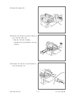
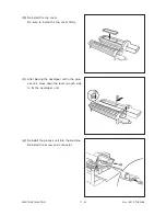
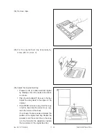
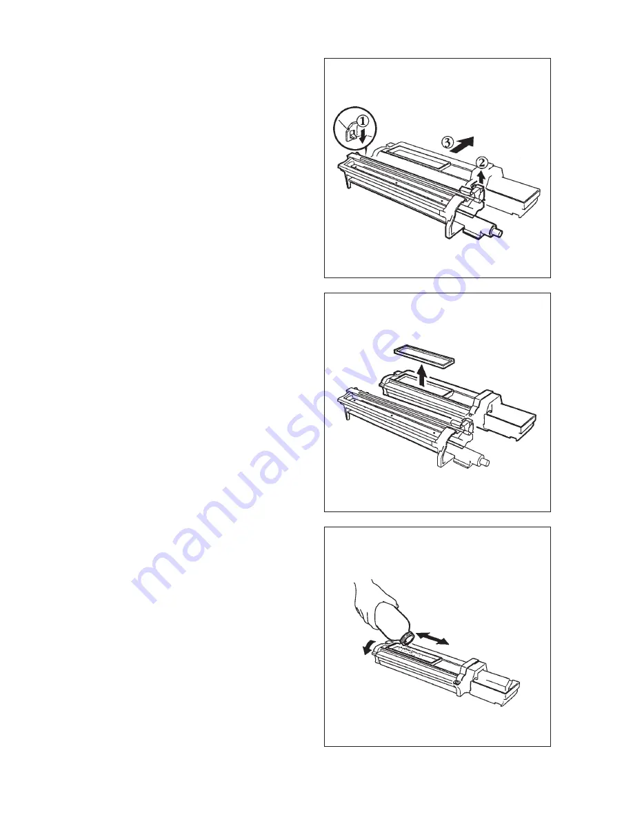
(17) Place the process unit on a flat surface.
Raise the lever located on each side of the
process unit in the direction of the arrow.
.
Remove the developer unit from the
process unit.
Note: If the photoconductor is exposed to fluo-
rescent light or external light for long
time, it may suffer from light-caused
fatigue. So, be sure to cover the process
unit with, for example, a suitable cloth.
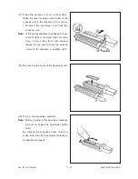
(18) Remove the top cover of the developer unit.
(19) Pour in the developer material.
Note: Before pouring in the developer material,
be sure to shake the developer bottle
fully.
By rotating the magnetic roller, check to
make sure that the developer material is
transported properly.
Содержание 3560
Страница 20: ...Nov 1997 TOSHIBA 2 13 3560 70 GENERAL 2 3 Wire Harness Location Diagram A Location diagram for upper unit ...
Страница 21: ...3560 70 GENERAL 2 14 Nov 1997 TOSHIBA B Location diagram for lower unit ...
Страница 72: ...Nov 1997 TOSHIBA 13 25 3560 70 CIRCUIT DIAGRAMS 13 3 Power Supply Circuit PS ACC A 115 V ...
Страница 73: ...3560 70 CIRCUIT DIAGRAMS 13 26 Nov 1997 TOSHIBA B 230 V ...
Страница 77: ...Nov 1997 TOSHIBA 15 1 3560 70 PC BOARD 15 PC BOARD ASSEMBLY 15 1 PWA LGC ...
Страница 78: ...3560 70 PC BOARD 15 2 Nov 1997 TOSHIBA 15 2 PWA PNL ...
Страница 79: ...Nov 1997 TOSHIBA 15 3 3560 70 PC BOARD 15 3 PWA KEY KEY1 KEY2 ...
Страница 80: ...3560 70 PC BOARD 15 4 Nov 1997 TOSHIBA 15 4 PWA ERS ...
Страница 81: ...Nov 1997 TOSHIBA 15 5 3560 70 PC BOARD 15 5 PS ACC A 1 115V ...
Страница 82: ...3560 70 PC BOARD 15 6 Nov 1997 TOSHIBA A 2 230V ...


