background image

SLUU131A – September 2002 – Revised February 2003

10

TPS40001 Based Converter Delivers 10-A Output

5

PowerPAD  Packaging

The TPS4000X family is available in the DGQ version of TI’s PowerPAD

t

 thermally enhanced package. In the

PowerPAD

t

, a thermally conductive epoxy is utilized to attach the integrated circuit die to the leadframe die

pad, which is exposed on the bottom of the completed package. The leadframe die pad can be soldered to the
PCB using standard solder flow techniques when maximum heat dissipation is required. However, depending
on power dissipation requirements, the PowerPAD

t

 may not need to soldered to the PCB.

The thermally conductive epoxy bonding the circuit die to the leadframe die pad causes a high resistance from
the leadframe die pad to the device ground pin 5. When the PowerPad

t

 package is soldered to the PCB, the

leadframe die pad can be connected to ground (pin 5), but this is not required. The leadframe die pad should
not be connected to other potentials in the circuit.

The PowerPAD

t

 package helps to keep the junction temperature rise relatively low even with the power

dissipation inherent in the onboard MOSFET drivers. This power loss is proportional to switching frequency,
drive voltage, and the gate charge needed to enhance the N-channel MOSFETs. Effective heat removal allows
the use of ultra small packaging while maintaining high component reliability.

To effectively remove heat from the PowerPAD

t

 package, a thermal land should be provided directly

underneath the package. This thermal land usually has vias that help to spread heat to internal copper layers
and/or the opposite side of the PCB. The vias should not have thermal reliefs that are often used on ground
planes, because this reduces the copper area to transfer heat. Additionally, the vias should be small enough
so that the holes are effectively plugged when plated. This prevents the solder from wicking away from the
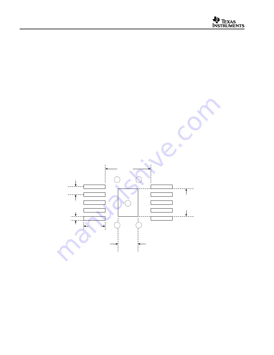
connection between the PCB surface and the bottom of the part. A typical footprint pattern is shown in Figure 2,
but does not include the additional copper plane which includes the vias above and below the device.

2.92mm
(0.115”)

0.5mm

(0.0197”)

0.28mm

(0.011”)

1.40mm

(0.055”)

Via Dia.

0.33mm
(0.013”)

Miminum

PowerPad ”X”

1.3mm

(0.050”)

Minimum

PowerPad ”Y”

1.7mm

(0.068”)

Figure 3. PowerPAD

t

 PCB Layout Guidelines

The Texas Instrument document, PowerPAD

t

 Thermally Enhanced Package Application Report (Texas

Instrument Literature Number SLMA002) should be consulted for more information on the PowerPAD

t

package. This report offers in-depth information on the package, assembly and rework techniques, and
illustrative examples of the thermal performance of the PowerPAD

t

 package.

Содержание TPS40001

Страница 1: ...User s Guide TPS40001 Based Converter Delivers 10 A Output User s Guide ...

Страница 2: ...e handling or use of the goods Please be aware that the products received may not be regulatory compliant or agency certified FCC UL CE etc Due to the open construction of the product it is the user s responsibility to take any and all appropriate precautions with regard to electrostatic discharge EXCEPT TO THE EXTENT OF THE INDEMNITY SET FORTH ABOVE NEITHER PARTY SHALL BE LIABLE TO THE OTHER FOR ...

Страница 3: ...certainty as to the load specification please contact a TI field representative During normal operation some circuit components may have case temperatures greater than 50 C The EVM is designed to operate properly with certain components above 50 C as long as the input and output ranges are maintained These components include but are not limited to linear regulators switching transistors pass trans...

Страница 4: ... to reduce conduction losses and increase silicon device utilization Predictive Gate Drive technology controls the delay from main switch turn off to synchronous rectifier turn on and also the delay from rectifier turn off to main switch turn on This allows minimization of the losses in the MOSFET body diodes both conduction and reverse recovery This design note provides details on a buck converte...

Страница 5: ...SLUU131A September 2002 Revised February 2003 5 TPS40001 Based Converter Delivers 10 A Output 3 Schematic Figure 1 Application Diagram for the TPS40002 3 ...

Страница 6: ...ns arising from crossing the DCM boundary A standard value of 1 µH with a resistance of 3 5 mΩ is selected At full load the power loss is only 0 35 W which is only 1 4 of the 25 W output power 4 3 Input Capacitor Selection Bulk input capacitor selection is based on allowable input voltage ripple and required RMS current carrying capability In typical buck converter applications the converter is fe...

Страница 7: ...ce runs at a high duty cycle and needs to have a low RDS on to keep conduction losses low and an 8 mΩ device with a maximum gate charge of 30 nC is selected The same device is fitted in the bottom switch location to achieve high efficiency 4 6 Short Circuit Protection The TPS40003 implements short circuit protection by comparing the voltage across the topside MOSFET while it is on to a voltage dro...

Страница 8: ...ation because the 1 µF is effectively out of the picture at these relatively low frequencies The feedback compensation network is implemented to provide two zeroes and three poles The first pole is placed near the origin to improve dc regulation The first zero is placed below fC at 2 2 kHz in equation 9 fz1 1 2 p ǒR6 R7 Ǔ C15 The second zero is placed at 18 kHz shown in equation 10 fz2 1 2 p R4 C7...

Страница 9: ...noisy An R C network fitted between this node and ground can help reduce ringing and voltage overshoot on Q2 This ringing noise should be minimized to prevent it from confusing the control circuitry which is monitoring this node for current limit Predictive Gate Drivet and DCM control functions As a starting point the snubber capacitor C12 is generally chosen to be 5 to 8 times larger than the par...

Страница 10: ...charge needed to enhance the N channel MOSFETs Effective heat removal allows the use of ultra small packaging while maintaining high component reliability To effectively remove heat from the PowerPADt package a thermal land should be provided directly underneath the package This thermal land usually has vias that help to spread heat to internal copper layers and or the opposite side of the PCB The...

Страница 11: ...ormance Data 6 1 Test Setup LOAD DVM2 DVM1 SCOPE Load adjustable from 0 10Amps GND VOUT VIN GND SLUP183A J1 J2 TP6 TP5 TP7 TP1 TP3 TP2 TP4 dc power supply adjustable from 0 V to 5 V Input wires 16 gauge or larger as short as feasible Output wires 16 gauge or larger as short as feasible IIN IOUT Figure 4 Test Setup ...

Страница 12: ...sured efficiency The input and output voltages are measured on the PCB as shown in the test diagram to avoid the losses associated with the input and output connectors Efficiency EFFICIENCY vs OUTPUT CURRENT IOUT Output Current A 50 55 60 65 70 75 80 85 90 95 100 0 00 2 00 6 00 8 00 10 00 4 00 Figure 5 Figure 6 shows the switch node at VIN 5 V and IOUT 10 A As the picture indicates there is almost...

Страница 13: ...hows the output voltage ripple at high VIN and full load which is the worst case condition for output voltage ripple t Time 1 µs div 10 mV div OUTPUT VOLTAGE RIPPLE Figure 7 Figure 8 shows the transient response with a 50 load step from 2 5 A to 7 5 A t Time 20 µs div 50 mV div TRANSIENT RESPONSE Figure 8 ...

Страница 14: ...131A September 2002 Revised February 2003 14 TPS40001 Based Converter Delivers 10 A Output 7 PCB Layout The PCB top assembly and copper layers are shown in Figures 9 through 11 Figure 9 Figure 10 Figure 11 ...

Страница 15: ...805 Panasonic ECJ 2YB1A105K C7 1 Ceramic 1 5 nF 50 V X7R 10 805 Vishay VJ0805Y152KXAAT C8 C9 2 POSCAP 470 µF 4 V 10 mΩ 20 7343 D Sanyo 4TPD470M Terminal Block J1 J2 2 4 pin 15 A 5 1 mm 291126 OST ED2227 Inductor L1 1 Inductor SMT 1 µH 15 A 3 5 mΩ 0 51 x 0 51 Vishay IHLP 5050CE 01 MOSFET Q1 Q2 2 MOSFET N channel 12 V 17 A 5 5 mΩ SO8 Siliconix Si4866DY Resistor R1 R5 1 Chip 1 8 Ω 1 10 W 5 805 Std St...

Страница 16: ...nt that any license either express or implied is granted under any TI patent right copyright mask work right or other TI intellectual property right relating to any combination machine or process in which TI products or services are used Information published by TI regarding third party products or services does not constitute a license from TI to use such products or services or a warranty or end...

Отзывы: