background image

User's Guide

SPRU997C – December 2009

Universal Asynchronous Receiver/Transmitter (UART)

1

Introduction

This document describes the universal asynchronous receiver/transmitter (UART) peripheral in the
TMS320DM643x Digital Media Processor (DMP) .

1.1

Purpose of the Peripheral

The UART peripheral is based on the industry standard TL16C550 asynchronous communications
element, which in turn is a functional upgrade of the TL16C450. Functionally similar to the TL16C450 on
power up (single character or TL16C450 mode), the UART can be placed in an alternate FIFO
(TL16C550) mode. This relieves the CPU of excessive software overhead by buffering received and
transmitted characters. The receiver and transmitter FIFOs store up to 16 bytes including three additional
bits of error status per byte for the receiver FIFO.

The UART performs serial-to-parallel conversions on data received from a peripheral device and
parallel-to-serial conversion on data received from the CPU. The CPU can read the UART status at any
time. The UART includes control capability and a processor interrupt system that can be tailored to
minimize software management of the communications link.

The UART includes a programmable baud generator capable of dividing the UART input clock by divisors
from 1 to 65 535 and producing a 16 × reference clock for the internal transmitter and receiver logic. For
detailed timing and electrical specifications for the UART, see the device specific data manual.

1.2

Features

The UART peripheral has the following features:

Programmable baud rates up to 128 kbps (frequency pre-scale values from 1 to 65535)

Fully programmable serial interface characteristics:

5, 6, 7, or 8-bit characters

Even, odd, or no PARITY bit generation and detection

1, 1.5, or 2 STOP bit generation

16-byte depth transmitter and receiver FIFOs:

The UART can be operated with or without the FIFOs

1, 4, 8, or 14 byte selectable receiver FIFO trigger level for autoflow control and DMA

DMA signaling capability for both received and transmitted data

CPU interrupt capability for both received and transmitted data

Operates in little-endian mode

False START bit detection

Line break generation and detection

Internal diagnostic capabilities:

Loopback controls for communications link fault isolation

Break, parity, overrun, and framing error simulation

Programmable autoflow control using CTS and RTS signals (not supported on all UARTs. See the
device-specific data manual for supported features.)

Modem control functions using CTS and RTS signals (not supported on all UARTs. See the
device-specific data manual for supported features.)

7

SPRU997C – December 2009

Universal Asynchronous Receiver/Transmitter (UART)

Submit Documentation Feedback

Copyright © 2009, Texas Instruments Incorporated

Содержание TMS320DM643x

Страница 1: ...TMS320DM643x DMP Universal Asynchronous Receiver Transmitter UART User s Guide Literature Number SPRU997C December 2009...

Страница 2: ...2 SPRU997C December 2009 Submit Documentation Feedback Copyright 2009 Texas Instruments Incorporated...

Страница 3: ...2 12 Emulation Considerations 20 2 13 Exception Processing 21 3 Registers 21 3 1 Receiver Buffer Register RBR 22 3 2 Transmitter Holding Register THR 23 3 3 Interrupt Enable Register IER 24 3 4 Inter...

Страница 4: ...r RBR 22 10 Transmitter Holding Register THR 23 11 Interrupt Enable Register IER 24 12 Interrupt Identification Register IIR 25 13 FIFO Control Register FCR 27 14 Line Control Register LCR 28 15 Modem...

Страница 5: ...n 26 12 FIFO Control Register FCR Field Descriptions 27 13 Line Control Register LCR Field Descriptions 28 14 Relationship Between ST EPS and PEN Bits in LCR 29 15 Number of STOP Bits Generated 29 16...

Страница 6: ...S320DM643x DMP DSP Subsystem Reference Guide Describes the digital signal processor DSP subsystem in the TMS320DM643x Digital Media Processor DMP SPRU983 TMS320DM643x DMP Peripherals Overview Referenc...

Страница 7: ...535 and producing a 16 reference clock for the internal transmitter and receiver logic For detailed timing and electrical specifications for the UART see the device specific data manual 1 2 Features...

Страница 8: ...ing CTS and RTS Supported 1 Autoflow control using CTS and RTS Supported 1 DTR and DSR Not supported Ring indication Not supported Carrier detection Not supported Single character transfer mode mode 0...

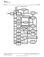
Страница 9: ...l Logic S e l e c t Data Bus Buffer RX TX Peripheral Bus S e l e c t Receiver Shift Register Receiver Timing and Control Transmitter Timing and Control Transmitter Shift Register Control Logic 16 8 8...

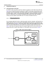
Страница 10: ...ed bit lasts 16 BCLK cycles When the UART is receiving the bit is sampled in the 8th BCLK cycle The formula to calculate the divisor is 1 Two 8 bit register fields DLH and DLL called divisor latches h...

Страница 11: ...e 3 Relationships Between Data Bit BCLK and UART Input Clock Table 2 Baud Rate Examples for 27 MHz UART Input Clock Baud Rate Divisor Value Actual Baud Rate Error 2400 703 2400 427 0 018 4800 352 4794...

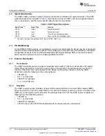
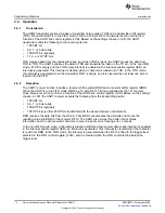
Страница 12: ...ta manual to determine how pin multiplexing affects the UART 2 4 Protocol Description 2 4 1 Transmission The UART transmitter section includes a transmitter hold register THR and a transmitter shift r...

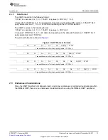
Страница 13: ...formats are shown in Figure 4 Figure 4 UART Protocol Formats D0 D1 D2 D3 D4 PARITY STOP1 Transmit Receive for 5 bit data parity Enable 1 STOP bit D0 D1 D2 D3 D4 D5 PARITY STOP1 Transmit Receive for 6...

Страница 14: ...eiver buffer register RBR When the UART is in the FIFO mode RBR is a 16 byte FIFO Timing is supplied by the 16 receiver clock Receiver section control is a function of the UART line control register L...

Страница 15: ...receiver time out interrupt occurs if all of the following conditions exist At least one character is in the FIFO The most recent character was received more than four continuous character times ago...

Страница 16: ...error and OE overrun error bits specify which error or errors have occurred The DR data ready bit is set as long as there is at least one byte in the receiver FIFO Also in the FIFO poll mode The inter...

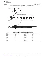
Страница 17: ...top the transmitter from sending the following byte CTS must be released before the middle of the last STOP bit that is currently being sent see Figure 7 When flow control is enabled CTS level changes...

Страница 18: ...priate values to the FIFO control register FCR The FIFOEN bit in FCR must be set first before the other bits in FCR are configured 5 Choose the desired protocol settings by writing the appropriate val...

Страница 19: ...s not respond to the FIFO trigger level The DR bit only indicates the presence or absence of unread characters RTOINT Receiver time out condition in the FIFO mode only The receiver time out interrupt...

Страница 20: ...miss the event and unless the UART generates a new event no data transfer will occur 2 11 Power Management The UART peripheral can be placed in reduced power modes to conserve power during periods of...

Страница 21: ...one address When the DLAB bit in LCR is 0 reading from the address gives the content of RBR and writing to the address modifies THR When DLAB 1 all accesses at the address read or modify DLL DLL can...

Страница 22: ...hen the FIFO is filled to the trigger level selected in the FIFO control register FCR and it is cleared when the FIFO contents drop below the trigger level Access considerations RBR THR and DLL share...

Страница 23: ...terrupt is generated when the transmitter FIFO is empty and it is cleared when at least one byte is loaded into the FIFO Access considerations RBR THR and DLL share one address To load THR write 0 to...

Страница 24: ...GEND R W Read Write R Read only n value after reset Table 9 Interrupt Enable Register IER Field Descriptions Bit Field Value Description 31 4 Reserved 0 Reserved 3 Reserved 0 Reserved This bit must al...

Страница 25: ...e content of IIR and writing to the address modifies FCR Figure 12 Interrupt Identification Register IIR 31 16 Reserved R 0 15 8 7 6 5 4 3 1 0 Reserved FIFOEN Reserved INTID IPEND R 0 R 0 R 0 R 0 R 1...

Страница 26: ...tion management register PWREMU_MGMT is loaded with 0 3 0 0 1 0 Transmitter holding Non FIFO mode Transmitter holding A character is written to the register empty register THR is empty transmitter hol...

Страница 27: ...erved 3 DMAMODE1 DMA MODE1 enable if FIFOs are enabled Always write 1 to DMAMODE1 After a hardware reset change DMAMODE1 from 0 to 1 DMAMOD1 1 is a requirement for proper communication between the UAR...

Страница 28: ...he address shared by RBR THR and DLL the CPU can read from and write to DLL At the address shared by IER and DLH the CPU can read from and write to DLH 6 BC Break control 0 Break condition is disabled...

Страница 29: ...the WLS bit determines the number of STOP bits 0 5 bits 1h 6 bits 2h 7 bits 3h 8 bits Table 14 Relationship Between ST EPS and PEN Bits in LCR ST Bit EPS Bit PEN Bit Parity Option x x 0 Parity disabl...

Страница 30: ...do not support this feature see the device specific data manual for supported features If this feature is not available this bit is reserved and should be cleared to 0 0 Autoflow control is disabled...

Страница 31: ...error or break indicator in the receiver FIFO 6 TEMT Transmitter empty TEMT indicator In non FIFO mode 0 Either the transmitter holding register THR or the transmitter shift register TSR contains a da...

Страница 32: ...ected with the character at the top of the receiver FIFO 2 PE Parity error PE indicator A parity error occurs when the parity of the received character does not match the parity selected with the EPS...

Страница 33: ...e in DLH and DLL DLH holds the most significant bits of the divisor and DLL holds the least significant bits of the divisor These divisor latches must be loaded during initialization of the UART in or...

Страница 34: ...rator Maximum baud rate is 128 kbps Figure 18 Divisor MSB Latch DLH 31 16 Reserved R 0 15 8 7 0 Reserved DLH R 0 R W 0 LEGEND R W Read Write R Read only n value after reset Table 19 Divisor MSB Latch...

Страница 35: ...ter 1 PID1 Field Descriptions Bit Field Value Description 31 16 Reserved 0 Reserved 15 8 CLS Identifies class of peripheral 1 Serial port 7 0 REV Identifies revision of peripheral 1 Current revision o...

Страница 36: ...the transmitter 0 Transmitter is disabled and in reset state 1 Transmitter is enabled 13 URRST UART receiver reset Resets and enables the receiver 0 Receiver is disabled and in reset state 1 Receiver...

Страница 37: ...ce the previous version of this document Table 23 Document Revision History Reference Additions Modifications Deletions Section 2 1 Changed first paragraph 37 SPRU997C December 2009 Revision History S...

Страница 38: ...ce TI is not responsible or liable for any such statements TI products are not authorized for use in safety critical applications such as life support where a failure of the TI product would reasonabl...

Отзывы: