


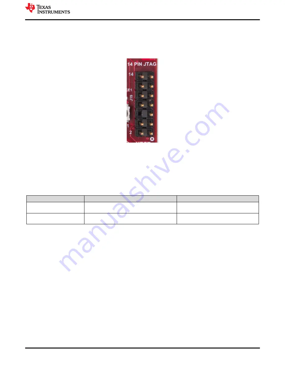
2.7.6 TI 14-Pin JTAG Connector (J19)
This connector provides a JTAG interface shown in
for debug and development through external
XDS emulators. To use this interface, the JTAG lines to the onboard emulator (XDS110) must be disconnected;
this is done with S1 (12th position of DIP switch should be open), and the external emulator on the MIPI 60-pin
connector also must be disconnected.
Figure 2-21. 14-Pin JTAG Connector
2.7.7 CAN Connector (J1 and J2)
The J1 and J2 connectors shown in
provide the CAN_L and CAN_H signals from the onboard CAND-
FD transceiver (TCAN1042HGVDRQ1) and CAN transceiver (SN65HVDA540QDR) independently, as shown in
. These signals are wired to the CAN bus after muxing with the SPI interface signals; one of the two
paths must be selected. Two CANs are selected by closing the switch S1 (1st position of switch to be ON).
Table 2-8. CAN Connectivity
Pin Description
Device Interface
Connector on Board
SPI_CS1
SPI_CLK1
CAN2_TX
CAN2_RX
J2 pin 1 (CAN2 corresponds to Regular CAN)
J2 pin 3
MISO_1
MOSI_1
CAN1_TX
CAN1_RX
J1 pin 1 (CAN1 corresponds to CANFD)
J1 pin 3
MMWAVEICBOOST
SWRU546D – OCTOBER 2018 – REVISED NOVEMBER 2020
mmWaveICBoost and Antenna Module
25
Copyright © 2020 Texas Instruments Incorporated


