LM4910
SNAS151G – MAY 2004 – REVISED MARCH 2007
www.ti.com
POWER SUPPLY BYPASSING
As with any amplifier, proper supply bypassing is important for low noise performance and high power supply
rejection. The capacitor location on the power supply pins should be as close to the device as possible.
Typical applications employ a 3.3V regulator with 10µF tantalum or electrolytic capacitor and a ceramic bypass
capacitor which aid in supply stability. This does not eliminate the need for bypassing the supply nodes of the
LM4910. A bypass capacitor value in the range of 0.1µF to 1µF is recommended for C
S
.
MICRO POWER SHUTDOWN
The voltage applied to the SHUTDOWN pin controls the LM4910's shutdown function. Activate micro-power
shutdown by applying a logic-low voltage to the SHUTDOWN pin. When active, the LM4910's micro-power
shutdown feature turns off the amplifier's bias circuitry, reducing the supply current. The trigger point is
0.4V(max) for a logic-low level, and 1.5V(min) for a logic-high level. The low 0.1µA(typ) shutdown current is
achieved by applying a voltage that is as near as ground as possible to the SHUTDOWN pin. A voltage that is
higher than ground may increase the shutdown current.
There are a few ways to control the micro-power shutdown. These include using a single-pole, single-throw
switch, a microprocessor, or a microcontroller. When using a switch, connect an external 100k
Ω
pull-up resistor
between the SHUTDOWN pin and V
DD
. Connect the switch between the SHUTDOWN pin and ground. Select
normal amplifier operation by opening the switch. Closing the switch connects the SHUTDOWN pin to ground,
activating micro-power shutdown. The switch and resistor guarantee that the SHUTDOWN pin will not float. This
prevents unwanted state changes. In a system with a microprocessor or microcontroller, use a digital output to
apply the control voltage to the SHUTDOWN pin. Driving the SHUTDOWN pin with active circuitry eliminates the
pull-up resistor.
SELECTING EXTERNAL COMPONENTS
Selecting proper external components in applications using integrated power amplifiers is critical to optimize
device and system performance. While the LM4910 is tolerant of external component combinations,
consideration to component values must be used to maximize overall system quality.
The LM4910 is unity-gain stable which gives the designer maximum system flexibility. The LM4910 should be
used in low gain configurations to minimize THD+N values, and maximize the signal to noise ratio. Low gain
configurations require large input signals to obtain a given output power. Input signals equal to or greater than
1V
rms
are available from sources such as audio codecs. Very large values should not be used for the gain-setting
resistors. Values for R
i
and R
f
should be less than 1M
Ω
. Please refer to the section, Audio Power Amplifier
Design, for a more complete explanation of proper gain selection
Besides gain, one of the major considerations is the closed-loop bandwidth of the amplifier. To a large extent, the
bandwidth is dictated by the choice of external components shown in
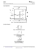
Figure 1
. The input coupling capacitor, C
i
,
forms a first order high pass filter which limits low frequency response. This value should be chosen based on
needed frequency response and turn-on time.
SELECTION OF INPUT CAPACITOR SIZE
Amplifiying the lowest audio frequencies requires a high value input coupling capacitor, C
i
. A high value capacitor
can be expensive and may compromise space efficiency in portable designs. In many cases, however, the
headphones used in portable systems have little ability to reproduce signals below 60Hz. Applications using
headphones with this limited frequency response reap little improvement by using a high value input capacitor.
In addition to system cost and size, turn-on time is affected by the size of the input coupling capacitor Ci. A larger
input coupling capacitor requires more charge to reach its quiescent DC voltage. This charge comes from the
output via the feedback Thus, by minimizing the capacitor size based on necessary low frequency response,
turn-on time can be minimized. A small value of Ci (in the range of 0.1µF to 0.39µF), is recommended.
12
Submit Documentation Feedback
Copyright © 2004–2007, Texas Instruments Incorporated
Product Folder Links:
LM4910
Содержание LM4910 Boomer
Страница 25: ...PACKAGE OPTION ADDENDUM www ti com 9 Aug 2013 Addendum Page 2 ...
Страница 28: ......
Страница 29: ...MECHANICAL DATA NGP0008A www ti com LQB08A Rev B ...


