LM4910
www.ti.com
SNAS151G – MAY 2004 – REVISED MARCH 2007
OUTPUT TRANSIENT ('CLICK AND POPS') ELIMINATED
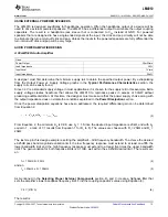
The LM4910 contains advanced circuitry that virtually eliminates output transients ('clicks and pops'). This
circuitry prevents all traces of transients when the supply voltage is first applied or when the part resumes
operation after coming out of shutdown mode. The LM4910 remains in a muted condition until there is sufficient
input signal magnitude (>5mV
RMS
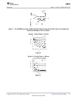
, typ) to mask any remaining transient that may occur. Figure 2 shows the
LM4910's lack of transients in the differential signal (Trace B) across a 320 load. The LM4910's active-low
SHUTDOWN pin is driven by the logic signal shown in Trace A. Trace C is the V
O1
output signal and Trace D is
the V
O3
output signal.
To ensure optimal click and pop performance under low gain configurations (less than 0dB), it is critical to
minimize the RC combination of the feedback resistor R
F
and stray input capacitance at the amplifier inputs. A
more reliable way to lower gain or reduce power delivered to the load is to place a current limiting resistor in
series with the load as explained in the Minimizing Output Noise / Reducing Output Power section.
AMPLIFIER CONFIGURATION EXPLANATION
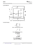
As shown in
Figure 1
, the LM4910 has three operational amplifiers internally. Two of the amplifier's have
externally configurable gain while the other amplifier is internally fixed at the bias point acting as a unity-gain
buffer. The closed-loop gain of the two configurable amplifiers is set by selecting the ratio of R
f
to R
i
.
Consequently, the gain for each channel of the IC is
A
V
= -(R
f
/R
i
)
(1)
By driving the loads through outputs V
O1
and V
O2
with V
O3
acting as a buffered bias voltage the LM4910 does not
require output coupling capacitors. The typical single-ended amplifier configuration where one side of the load is
connected to ground requires large, expensive output coupling capacitors.
A configuration such as the one used in the LM4910 has a major advantage over single supply, single-ended
amplifiers. Since the outputs V
O1
, V
O2
, and V
O3
are all biased at V
REF
= 1.58V, no net DC voltage exists across
each load. This eliminates the need for output coupling capacitors that are required in a single-supply, single-
ended amplifier configuration. Without output coupling capacitors in a typical single-supply, single-ended
amplifier, the bias voltage is placed across the load resulting in both increased internal IC power dissipation and
possible loudspeaker damage.
POWER DISSIPATION
Power dissipation is a major concern when designing a successful amplifier. A direct consequence of the
increased power delivered to the load by a bridge amplifier is an increase in internal power dissipation. The
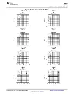
maximum power dissipation for a given application can be derived from the power dissipation graphs or from
Equation 1.
P
DMAX
= 4(V
DD
)
2
/ (
π
2
R
L
)
(2)
It is critical that the maximum junction temperature T
JMAX
of 150°C is not exceeded. Since the typical application
is for headphone operation (32
Ω
impedance) using a 3.3V supply the maximum power dissipation is only
138mW. Therefore, power dissipation is not a major concern.
Copyright © 2004–2007, Texas Instruments Incorporated
Submit Documentation Feedback
11
Product Folder Links:
LM4910
Содержание LM4910 Boomer
Страница 25: ...PACKAGE OPTION ADDENDUM www ti com 9 Aug 2013 Addendum Page 2 ...
Страница 28: ......
Страница 29: ...MECHANICAL DATA NGP0008A www ti com LQB08A Rev B ...


