background image

IADJ

EN

CSN

LM3409HV

UVLO

V

IN

VCC

COFF

GND

CSP

C4

R6

PGATE

C7

R8

R7

DAP

VIN

LED+

R9

1

2

3

4

5

6

7

8

9

10

PWM2

C1

C2

5V

R4

C9

R3

R2

R1

D1

L1

Q3

Q2

C3

C5

GND2

LED-

GND

VADJ

R10

C6

R11

C8

R5

D2

1

2

3

5

6

7

14

13

12

10

9

8

J2

J1

1

3

EN

Q1

U1

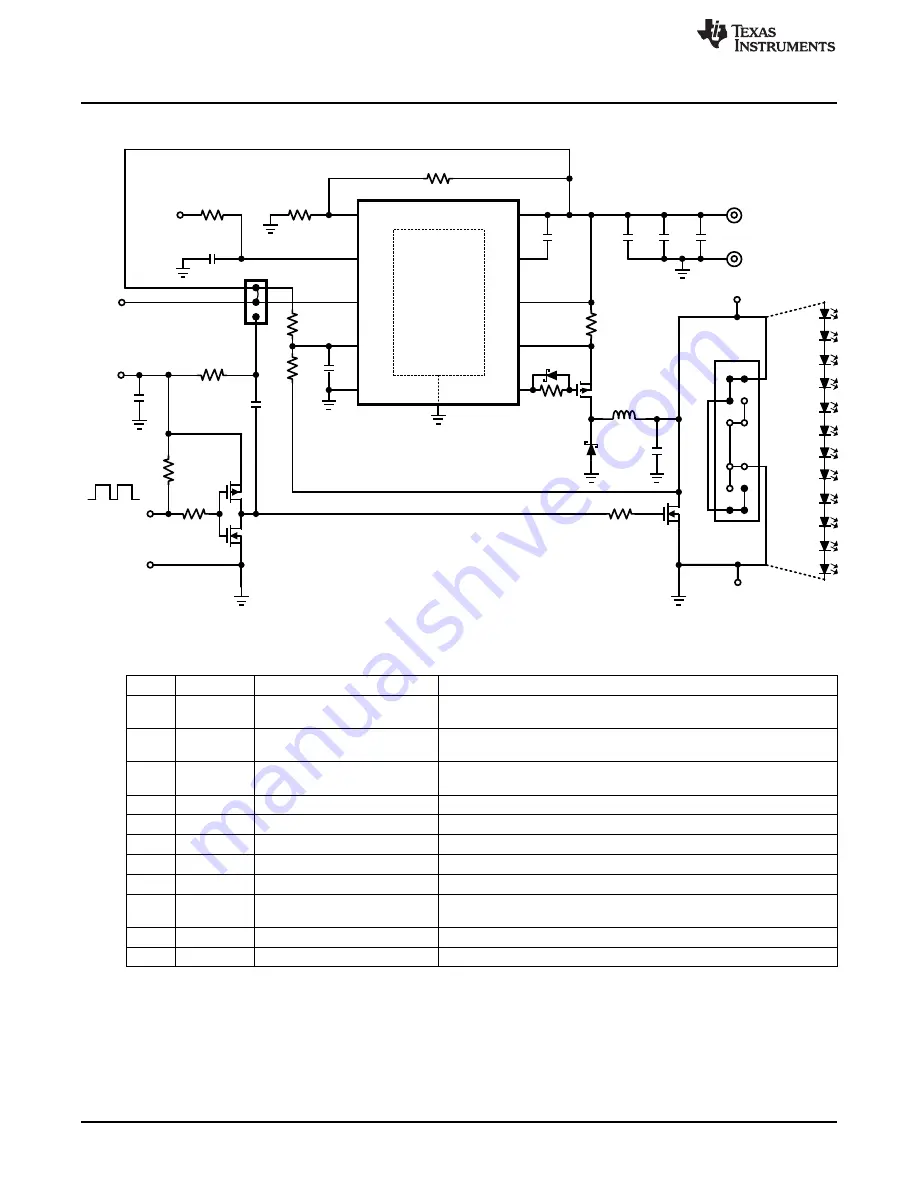
Schematic

www.ti.com

2

Schematic

3

Pin Descriptions

Pin(s)

Name

Description

Application Information

1

UVLO

Input under-voltage lockout

Connect to a resistor divider from V

IN

and GND. Turn-on threshold is

1.24V and hysteresis for turn-off is provided by a 22µA current source.

2

IADJ

Analog LED current adjust

Apply a voltage between 0 - 1.24V, connect a resistor to GND, or leave
open to set the current sense threshold voltage.

3

EN

Logic level enable /

Apply a voltage >1.74V to enable device, a PWM signal to dim, or a

PWM dimming

voltage <0.5V for low power shutdown.

4

COFF

Off-time programming

Connect resistor to V

O

, and capacitor to GND to set the off-time.

5

GND

Ground

Connect to the system ground.

6

PGATE

Gate drive

Connect to the gate of the external PFET.

7

CSN

Negative current sense

Connect to the negative side of the sense resistor.

8

CSP

Positive current sense

Connect to the positive side of the sense resistor (V

IN

).

9

VCC

V

IN

- referenced

Connect at least a 1µF ceramic capacitor to V

IN

. The regulator provides

linear regulator output

power for the PFET drive.

10

VIN

Input voltage

Connect to the input voltage.

DAP

DAP

Thermal pad on bottom of IC

Connect to pin 5 (GND). Place 4-6 vias from DAP to bottom GND plane.

2

AN-1953 LM3409HV Evaluation Board

SNVA390D – May 2009 – Revised May 2013

Submit Documentation Feedback

Copyright © 2009–2013, Texas Instruments Incorporated

Содержание LM3409HV

Страница 1: ...which is used to select the PWM dimming method The evaluation board has a right angle connector J2 which can mate with an external LED load board allowing for the LEDs to be mounted close to the driver This reduces potential ringing when there is no output capacitor Alternatively the LED and LED turrets can be used to connect the LED load This board can be easily modified to demonstrate other oper...

Страница 2: ... 1 74V to enable device a PWM signal to dim or a PWM dimming voltage 0 5V for low power shutdown 4 COFF Off time programming Connect resistor to VO and capacitor to GND to set the off time 5 GND Ground Connect to the system ground 6 PGATE Gate drive Connect to the gate of the external PFET 7 CSN Negative current sense Connect to the negative side of the sense resistor 8 CSP Positive current sense ...

Страница 3: ... Q3 NMOS 100V 7 5A FAIRCHILD FDS3672 1 D1 Schottky 100V 3A VISHAY SS3H10 E3 57T 1 L1 33 µH 20 3 2A TDK SLF12575T 330M3R2 2 R1 R2 1Ω 1 VISHAY CRCW06031R00FNEA 1 R3 10kΩ 1 VISHAY CRCW060310K0FKEA 1 R4 100Ω 1 VISHAY CRCW0603100RFKEA 1 R5 0Ω 1 VISHAY CRCW06030000Z0EA 1 R6 16 5kΩ 1 VISHAY CRCW060316K5FKEA 1 R7 6 98kΩ 1 VISHAY CRCW06036K98FKEA 1 R8 49 9kΩ 1 VISHAY CRCW060349K9FKEA 1 R9 0 15Ω 1 1W VISHAY...

Страница 4: ...out The two inner planes are GND and VIN Figure 2 Top Layer Figure 3 Bottom Layer 4 AN 1953 LM3409HV Evaluation Board SNVA390D May 2009 Revised May 2013 Submit Documentation Feedback Copyright 2009 2013 Texas Instruments Incorporated ...

Страница 5: ...sign Procedure 6 1 Specifications VIN 48V VIN MAX 75V VO 42V fSW 400kHz ILED 1 5A ΔiLED PP ΔiL PP 300mA ΔvIN PP 1 44V VTURN ON 10V VHYS 1 1V η 0 97 6 2 Nominal Switching Frequency Assume C7 470pF and η 0 97 Solve for R6 1 The closest 1 tolerance resistor is 16 5 kΩ therefore the actual tOFF and target fSW are 2 3 The chosen components from step 1 are 4 5 SNVA390D May 2009 Revised May 2013 AN 1953 ...

Страница 6: ...ign Procedure www ti com 6 3 Inductor Ripple Current Solve for L1 5 The closest standard inductor value is 33 µH therefore the actual ΔiL PP is 6 The chosen component from step 2 is 7 6 4 Average LED Current Determine IL MAX 8 Assume VADJ 1 24V and solve for R9 9 The closest 1 tolerance resistor is 0 15 Ω therefore the ILED is 10 The chosen component from step 3 is 11 6 5 Output Capacitance No out...

Страница 7: ...K x I V LED O x V 75 V V MAX IN MAX T www ti com Design Procedure 6 7 P Channel MOSFET Determine minimum Q1 voltage rating and current rating 18 19 A 100V 3 8A PFET is chosen with RDS ON 190mΩ and Qg 20nC Determine IT RMS and PT 20 21 The chosen component from step 6 is 22 6 8 Recirculating Diode Determine minimum D1 voltage rating and current rating 23 24 A 100V 3A diode is chosen with VD 750mV D...

Страница 8: ...nally It can be necessary to have an RC filter when using an external power supply in order to remove any high frequency noise or oscillations created by the power supply and the connecting cables The filter is chosen by assuming a standard value of C6 0 1µF and solving for a cut off frequency fC 2kHz 32 Since an exact fC is not critical a standard value of 1kΩ is used Section 8 shows a typical LE...

Страница 9: ...d to the PWM2 terminal the shunt dimming circuit is complete Q3 is the shunt dimFET which conducts the LED current when turned on and blocks the LED voltage when turned off Q3 needs to be fast and rated for VO and ILED For design flexibility a fast 100V 7 5A NFET is chosen Q2 is necessary to invert the PWM signal so it properly translates the duty cycle to the shunt dimming FET Q2 also needs to be...

Страница 10: ...xternal parallel FET dimming circuit will keep the inductor current close to its nominal value when Q3 is turned off This modification will ensure that the rise time of the LED current is only limited by the turn off time of the shunt FET as desired The following circuit additions allow for two different off times to occur When Q3 is off the standard off timer referenced from VO is set However whe...

Страница 11: ...ADJ R10 C6 R11 C8 R5 D2 1 2 3 5 6 7 14 13 12 10 9 8 J2 J1 1 3 EN Q1 U1 Two Off timers for Shunt FET dimming ROFF2 www ti com Shunt FET Circuit Modification Figure 5 Multiple off timers for shunt FET dimming circuit 11 SNVA390D May 2009 Revised May 2013 AN 1953 LM3409HV Evaluation Board Submit Documentation Feedback Copyright 2009 2013 Texas Instruments Incorporated ...

Страница 12: ... 7 6 5 4 3 2 1 0 1 2 8 2 4 2 0 1 6 1 2 0 8 0 4 0 0 0 4 ILED 2 és DIV 3 5 és VEN Typical Waveforms www ti com 8 Typical Waveforms TA 25 C VIN 48V and VO 42V Figure 6 20kHz 50 EN pin PWM dimming Figure 7 20kHz 50 EN pin PWM dimming rising edge Figure 8 100kHz 50 External FET PWM dimming Figure 9 100kHz 50 External FET PWM dimming rising edge 12 AN 1953 LM3409HV Evaluation Board SNVA390D May 2009 Rev...

Страница 13: ...R6 R9 L1 and C8 The RMS current rating of L1 should be at least 50 higher than the specified ILED Designs 3 and 5 are optimized for best analog dimming range while designs 1 2 and 4 are optimized for best PWM dimming range These are just examples however any combination of specifications can be achieved by following the Design Procedure in the LM3409 3409HV 3409Q 3409QHV PFET Buck Controller for H...

Страница 14: ...esponsible for compliance with all legal regulatory and safety related requirements concerning its products and any use of TI components in its applications notwithstanding any applications related information or support that may be provided by TI Buyer represents and agrees that it has all the necessary expertise to create and implement safeguards which anticipate dangerous consequences of failur...

Отзывы: