Texas Instruments AN-1622 LM49100 Скачать руководство пользователя страница 14

HPR

HPL

AGND

Application Information

www.ti.com

15

Application Information

15.1 Minimizing Click and Pop

To minimize the audible click and pop heard through a headphone, maximize the input signal through the
corresponding volume (gain) control registers and adjust the output amplifier gain accordingly to achieve
the your desired signal gain. For example, setting the output of the headphone amplifier to -24dB and
setting the input volume control gain to 24dB will reduce the output offset from 7mV (typical) to 2.2mV
(typical). This will reduce the audible click and pop noise significantly while maintaining a 0dB signal gain.

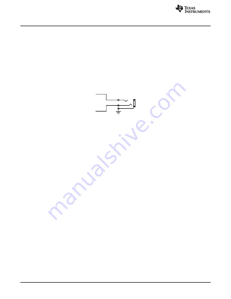
15.2 Signal Ground Noise

The LM49100 has proprietary suppression circuitry, which provides an additional -50dB (typical)
attenuation of the headphone ground noise and its incursion into the headphone. For optimum utilization
of this feature, the headphone jack ground should connect to the AGND (E3) bump.

Figure 18. Suppression Circuitry

15.3 I

2

C Pin Description

SDA: This is the serial data input pin.

SCL: This is the clock input pin.

ADDR: This is the address select input pin.

15.4 I

2

C Compatible Interface

The LM49100 uses a serial bus which conforms to the I

2

C protocol to control the chip's functions with two

wires: clock (SCL) and data (SDA). The clock line is uni-directional. The data line is bi-directional (open-
collector). The LM49100's I

2

C compatible interface supports standard (100kHz) and fast (400kHz) I

2

C

modes. In this discussion, the master is the controlling microcontroller and the slave is the LM49100.

The I

2

C address for the LM49100 is determined using the ADDR pin. The LM49100's two possible I

2

C chip

addresses are of the form 111110X

1

0 (binary), where X

1

= 0, if ADDR pin is logic LOW; and X

1

= 1, if

ADDR pin is logic HIGH. If the I

2

C interface is used to address a number of chips in a system, the

LM49100's chip address can be changed to avoid any possible address conflicts.

The bus format for the I

2

C interface is shown in

Figure 19

and the timing diagram is shown in

Figure 20

.

The bus format diagram is broken up into six major sections:

The "start" signal is generated by lowering the data signal while the clock signal is HIGH. The start
signal will alert all devices attached to the I

2

C bus to check the incoming address against their own

address.

The 8-bit chip address is sent next, most significant bit first. The data is latched in on the rising edge of
the clock. Each address bit must be stable while the clock level is HIGH.

After the last bit of the address bit is sent, the master releases the data line HIGH (through a pull-up
resistor). Then the master sends an acknowledge clock pulse. If the LM49100 has received the
address correctly, then it holds the data line LOW during the clock pulse. If the data line is not held
LOW during the acknowledge clock pulse, then the master should abort the rest of the data transfer to
the LM49100.

The 8 bits of data are sent next, most significant bit first. Each data bit should be valid while the clock
level is stable HIGH.

14

AN-1622 LM49100 Evaluation Board»

SNAA043A – October 2007 – Revised May 2013

Submit Documentation Feedback

Copyright © 2007–2013, Texas Instruments Incorporated

Содержание AN-1622 LM49100

Страница 1: ...pin and HPR pin carries the output signals from the two amplifiers and each of the other pins connecting to ground making this configuration single ended connections 6 Differential mono amplifier outp...

Страница 2: ...th a mono input signal The LM49100 features a 32 step digital volume control and ten distinct output modes The mixer volume control and device mode select are controlled through an I2 C compatible int...

Страница 3: ...d is an I2 C signal generation board and software With this board and the software the user can easily control the LM49100 s shutdown function mute and stereo volume control Figure 2 shows the softwar...

Страница 4: ...ation board VDDHP GND Headphone power supply for the headphone amplifier which creates split supplies for the positive voltage is converted by switch capacitor creating a negative voltage of equal mag...

Страница 5: ...udes controls for the amplifier s volume control individual channel shutdown and the mute function The control program s on screen user interface is shown in Figure 2 The Default button is used to ret...

Страница 6: ...r 0 1 F 0805 HPL 2 pin header 100 mil pitch 1x2 Header HPR 2 pin header 100 mil pitch 1x2 Header I2C 6 pin 6 pin header 100 mil pitch 2x3 Header Header Left Input 2 pin header 100 mil pitch 1x2 Header...

Страница 7: ...ration Board PCB Layout Figure 4 Top Overlay Figure 5 Top Layer 7 SNAA043A October 2007 Revised May 2013 AN 1622 LM49100 Evaluation Board Submit Documentation Feedback Copyright 2007 2013 Texas Instru...

Страница 8: ...yout www ti com Figure 6 Upper Inner Layer Figure 7 Lower Middle Layer 8 AN 1622 LM49100 Evaluation Board SNAA043A October 2007 Revised May 2013 Submit Documentation Feedback Copyright 2007 2013 Texas...

Страница 9: ...ion Board PCB Layout Figure 8 Bottom Layer Figure 9 Bottom Overlay 9 SNAA043A October 2007 Revised May 2013 AN 1622 LM49100 Evaluation Board Submit Documentation Feedback Copyright 2007 2013 Texas Ins...

Страница 10: ...5 respectively Typical THD N versus Output Power performance curves at VDD 3V 3 6V and 5V for 32 and 8 are shown in Figure 16 and Figure 17 respectively Figure 10 THD N vs Frequency Figure 11 THD N vs...

Страница 11: ...ti com Typical Demonstration Board Audio Performance Figure 16 THD N vs Output Power Figure 17 THD N vs Output Power RL 32 f 1kHz RL 8 f 1kHz BW 22kHz HP Mode 4 BW 22kHz LS Mode 1 11 SNAA043A October...

Страница 12: ...ed for extra headphone output attenuation Table 4 Output Mode Selection 1 Output Mode MC3 MC2 MC1 MC0 Handsfree Mono Output Right HP Output Left HP Output Number 0 0 0 0 0 SD SD SD 1 0 0 0 1 2 GM M SD...

Страница 13: ...0 1 0 13 5 19 5 12 0 1 0 1 1 12 18 13 0 1 1 0 0 10 5 16 5 14 0 1 1 0 1 9 15 15 0 1 1 1 0 7 5 13 5 16 0 1 1 1 1 6 12 17 1 0 0 0 0 4 5 10 5 18 1 0 0 0 1 3 9 19 1 0 0 1 0 1 5 7 5 20 1 0 0 1 1 0 6 21 1 0...

Страница 14: ...olling microcontroller and the slave is the LM49100 The I2 C address for the LM49100 is determined using the ADDR pin The LM49100 s two possible I2 C chip addresses are of the form 111110X10 binary wh...

Страница 15: ...I2 C Bus Format Figure 20 I2 C Timing Diagram 15 5 I2 C Interface Power Supply Pin VDDI2 C The LM49100 s I2 C interface is powered up through theVDD I2 C pin The LM49100 s I2 C interface operates at...

Страница 16: ...he single ended configuration its differential output doubles the voltage swing across the load Theoretically this produces four times the output power when compared to a single ended amplifier under...

Страница 17: ...emperature If these measures are insufficient a heat sink can be added to reduce JA The heat sink can be created using additional copper area around the package with connections to the ground pin s su...

Страница 18: ...ess shutdown function As discussed above choosing CIN no larger than necessary for the desired bandwidth helps minimize clicks and pops CB s value should be in the range of 4 to 5 times the value of C...

Страница 19: ...y 18 Revision History Rev Date Description 1 0 10 1907 Initial release 19 SNAA043A October 2007 Revised May 2013 AN 1622 LM49100 Evaluation Board Submit Documentation Feedback Copyright 2007 2013 Texa...

Страница 20: ...sponsible for compliance with all legal regulatory and safety related requirements concerning its products and any use of TI components in its applications notwithstanding any applications related inf...

Отзывы: