background image


T-Core 
User Manual


62 


www.terasic.com 

January 14, 2020 


2.


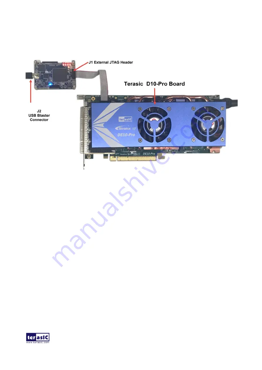
Connect the other end of the flat ribbon cable to the 2x5 JTAG header on the DE10-Pro board, 
see 

Figure 5-5

. 


Figure 5-5 The flat ribbon cable connected to the T-Core board 

3.


Using mini USB cable to connected J2 of the T-Core board and the host PC. 

4.


Power the DE10-Pro board. 

5.


Open  the  Quartus  programmer  on  the  host  PC,  press  "Hardware  Setup"  and  select  T-Core 
[USB-*].  Then  press  "Auto  Detect"  and  the  Stratix  10  FPGA  device  on  the  DE10-Pro  will 
appear in the window, as shown in 

Figure 5-6

. 

Содержание T-Core

Страница 1: ...T Core User Manual 1 www terasic com January 14 2020 ...

Страница 2: ... the Push buttons Switches and LEDs 16 2 4 Using WS2812B RGB LED 18 2 5 Using 2x6 TMD GPIO Expansion Headers 21 2 6 1x10 A D Converter and Analog Input 22 2 7 Using QSPI Flash 23 Chapter 3 Example Designs 25 3 1 T Core Factory Configuration 25 3 2 Control RGB LED in Nios II 28 3 3 Control External RGB LED in Nios II 31 3 4 ADC Measurement 33 3 5 RISC V 36 Chapter 4 Programming the Configuration Fl...

Страница 3: ...ng motor control drive analog to digital conversion and handheld devices the T Core MAX 10 FPGA is your best choice The T Core development board includes hardware such as on board USB Blaster II QSPI Flash ADC Header WS2812B RGB LEDs and 2x6 TMD expansion header By leveraging all of these capabilities the T Core is the perfect solution for showcasing evaluating and prototyping the true potential o...

Страница 4: ...e User Manual reference designs and device datasheets User can download this System CD from the web http T Core terasic com cd 1 1 3 3 L La ay yo ou ut t a an nd d C Co om mp po on ne en nt ts s This section presents the features and design characteristics of the board A photograph of the board is shown in Figure 1 2 and Figure 1 3 It depicts the layout of the board and indicates the location of t...

Страница 5: ...ided on the board F FP PG GA A D De ev vi ic ce e MAX 10 10M50DAF484C7G Device Integrated dual ADCs each ADC supports 1 dedicated analog input and 8 dual function pins 50K programmable logic elements 1 638 Kbits M9K Memory 5 888 Kbits user flash memory 144 18 18 Multiplier 4 PLLs P Pr ro og gr ra am mm mi in ng g a an nd d C Co on nf fi ig gu ur ra at ti io on n On Board USB Blaster II Mini USB co...

Страница 6: ...itches 2 Push Buttons with Debounced 4 WS2812B RGB LED P Po ow we er r 5V DC input from USB or external power connector 1 1 4 4 B Bl lo oc ck k D Di ia ag gr ra am m o of f t th he e B Bo oa ar rd d Figure 1 4 gives the block diagram of the board To provide maximum flexibility for the user all connections are made through the MAX 10 FPGA device Thus the user can configure the FPGA to implement any...

Страница 7: ... G Ge et tt ti in ng g H He el lp p Here are the addresses where you can get help if you encounter any problem Terasic Inc 9F No 176 Sec 2 Gongdao 5th Rd East Dist Hsinchu City 30070 Taiwan Email support terasic com Tel 886 3 5750 880 Web http T Core terasic com ...

Страница 8: ...ation you need to program the configuration data into the configuration flash memory CFM which provides non volatile storage for the bit stream The information is retained within CFM even if the T Core board is turned off When the board is powered on the configuration data in the CFM is automatically loaded into the MAX 10 FPGA JTAG Chain on T Core Board Figure 2 1 shows the JTAG interface of T Co...

Страница 9: ...Core SW2 2 is the JTAG chain switch for RISC V applications If it is turned off the application will not appear in the JTAG chain For more information about the RISC V application please refer to section 3 5 for more information Table 2 1 is the setting of SW2 and its function Table 2 1 MAX10 and RISC V JTAG Chain setting for SW2 SW2 Position Description MAX10 SW2 1 RISC V SW2 2 OFF OFF MAX10 and ...

Страница 10: ... by step 1 Open the Quartus Prime programmer please choose Tools Programmer The Programmer window opens See Figure 2 3 Figure 2 3 Programmer Window 2 Click Hardware Setup as circled in Figure 2 3 3 If it is not already turned on turn on the USB Blaster USB 0 option under currently selected hardware and click Close to close the window See Figure 2 4 ...

Страница 11: ...y 14 2020 Figure 2 4 Hardware Setting 4 Click Auto Detect to detect all the devices on the JTAG chain as circled in Figure 2 5 Figure 2 5 Detect FPGA device in JTAG mode 5 Select detected device associated with the board as circled in Figure 2 6 ...

Страница 12: ...T Core User Manual 11 www terasic com January 14 2020 Figure 2 6 Select 10M50DA device 6 FPGA is detected as shown in Figure 2 7 Figure 2 7 FPGA detected in Quartus Prime programmer ...

Страница 13: ...on the FPGA device and click Change File to open the sof file to be programmed as highlighted in Figure 2 8 Figure 2 8 Open the sof file to be programmed into the FPGA device 8 Open the output_files folder and select the sof file to be programmed as shown in Figure 2 9 ...

Страница 14: ...0 Figure 2 9 Select the sof file to be programmed into the FPGA device 9 Click Program Configure check box and then click Start button to download the sof file into the FPGA device as shown in Figure 2 10 Figure 2 10 Program sof file into the FPGA device ...

Страница 15: ...p Please refer to Chapter 4 Programming the Configuration Flash Memory CFM for the basic programming instruction on the configuration flash memory CFM Figure 2 11 High Level Overview of Internal Configuration for MAX 10 Devices Status LED The T Core development board includes board specific status LEDs to indicate board status Please refer to Table 2 2 for the description of the LED indicator Plea...

Страница 16: ... clock signals with low jitter The two 50MHz clock signals connected to the FPGA are used as clock sources for user logic One 24MHz clock signal is connected to the clock inputs of USB microcontroller of USB Blaster One 10MHz clock signal is connected to the PLL1 and PLL3 of FPGA the outputs of these two PLLs can drive ADC clock The associated pin assignment for clock inputs to FPGA I O pins is li...

Страница 17: ...igure 2 15 for the push buttons connected Table 2 4 list the pin assignment of user push buttons Figure 2 14 Connections between the push button and MAX 10 FPGA Figure 2 15 Switch debouncing Table 2 4 Pin Assignment of Push buttons Signal Name FPGA Pin No Description I O Standard KEY 0 PIN_AB9 Push button 0 3 3 V SCHMITT TRIGGER KEY 1 PIN_AA9 Push button 1 3 3 V SCHMITT TRIGGER User Defined Dip Sw...

Страница 18: ...nal Name FPGA Pin No Description I O Standard SW 0 PIN_AB16 Dip Switch 0 3 3 V LVTTL SW 1 PIN_Y16 Dip Switch 1 3 3 V LVTTL SW 2 PIN_V16 Dip Switch 2 3 3 V LVTTL SW 3 PIN_AB17 Dip Switch 3 3 3 V LVTTL User Defined LEDs There are also four user controllable LEDs connected to FPGA on the board Each LED is driven directly and individually by a pin on the MAX 10 FPGA driving its associated pin to a hig...

Страница 19: ...e four Color LED WS2812B with intelligent controller See Figure 2 18 and the four LED are connected in series controlled by one GPIO line The WS2812B is an intelligent control LED light source that the control circuit and RGB chip are integrated in a package of 5050 components It internal includes intelligent digital port data latch and signal reshaping amplification drive circuit Also includes a ...

Страница 20: ... T0H 0 code high voltage time 220ns 380ns T1H 1 code high voltage time 580ns 1µs T0L 0 code low voltage time 580ns 1µs T1L 1 code low voltage time 220ns 420ns RES Frame unit low voltage time 280µs The data transfer protocol of the WS281 use single NRZ communication mode As shown in Figure 2 21 after the pixel power on reset the DI port receive data from controller the first pixel collect initial 2...

Страница 21: ... Standard OB_LED_RGB_D PIN_D19 On Board RGB LED Data IN 3 3 V LVTTL EX_LED_RGB_D PIN_D18 RGB LED Data IN for External Header 3 3 V LVTTL Expansion Port In addition to the Built in four RGB LEDs on the T Core board two 3 pin headers JP3 and JP4 are reserved for user to expand more LED Users can purchase the commercially RGB LED Line Pipe in series to make the application more widely available See F...

Страница 22: ...veform to output Pin 3 is grounded Please note that if the external light strip is attached the ground of the light strip should be connected to this pin For detailed RGB LED and JP3 JP4 position please refer to Figure 2 22 simple connection method refer to Figure 2 23 Figure 2 22 JP3 JP4 and RGB LED Location Figure 2 23 An example of a color light bar connection for an external power supply 2 2 5...

Страница 23: ... LVTTL TMD_D 2 PIN_AA5 GPIO Connection 2 3 3 V LVTTL TMD_D 3 PIN_AB5 GPIO Connection 3 3 3 V LVTTL TMD_D 4 PIN_AB7 GPIO Connection 4 3 3 V LVTTL TMD_D 5 PIN_AA7 GPIO Connection 5 3 3 V LVTTL TMD_D 6 PIN_AB6 GPIO Connection 6 3 3 V LVTTL TMD_D 7 PIN_AA6 GPIO Connection 7 3 3 V LVTTL 2 2 6 6 1 1x x1 10 0 A A D D C Co on nv ve er rt te er r a an nd d A An na al lo og g I In np pu ut t The board has e...

Страница 24: ...ut Data 2 2 5 V LVTTL ADC_IN 3 PIN_J9 Analog Input Data 3 2 5 V LVTTL ADC_IN 4 PIN_J4 Analog Input Data 4 2 5 V LVTTL ADC_IN 5 PIN_H3 Analog Input Data 5 2 5 V LVTTL ADC_IN 6 PIN_K5 Analog Input Data 6 2 5 V LVTTL ADC_IN 7 PIN_K6 Analog Input Data 7 2 5 V LVTTL 2 2 7 7 U Us si in ng g Q QS SP PI I F Fl la as sh h The board supports a 64M bit serial NOR flash device for non volatile storage user da...

Страница 25: ...gnal Name FPGA Pin No Description I O Standard QSPI_FLASH_DATA 0 PIN_P21 FLASH Data 0 3 3 V LVTTL QSPI_FLASH_DATA 1 PIN_P18 FLASH Data 1 3 3 V LVTTL QSPI_FLASH_DATA 2 PIN_R18 FLASH Data 2 3 3 V LVTTL QSPI_FLASH_DATA 3 PIN_P20 FLASH Data 3 3 3 V LVTTL QSPI_FLASH_SCLK PIN_P19 FLASH Data Clock 3 3 V LVTTL QSPI_FLASH_CEN PIN_L22 FLASH Chip Enable 3 3 V LVTTL ...

Страница 26: ...ise it will lead to error in Nios II software Note Quartus Prime Standard v18 1 or later is required for all T Core demonstrations to support MAX 10 FPGA device 3 3 1 1 T T C Co or re e F Fa ac ct to or ry y C Co on nf fi ig gu ur ra at ti io on n The T Core board has a default configuration bit stream pre programmed which demonstrates some of the basic features onboard The setup required for this...

Страница 27: ...if the KEY0 is not pressed 5 WS2812 It is the WS2812 IC control IP it can control any WS2812 IC it contains two main parts TWO_PORT_RAM User can write in the R 7 0 G 7 0 B 7 0 data to control any one of RGB LEDs to be light as any colors For example user can set ram_wraddress 2 ram_data R 7 0 G 7 0 B 7 0 8 h00 8 hff 8 h00 to make the RGB LED3 light as Green then set the ram_wrclock to 0 1 0 the da...

Страница 28: ...monstration Setup and Instructions Connect the Mini USB connector J2 of the T Core board to the host PC with a USB cable and install the USB Blaster II driver if necessary Execute the demo batch file test bat from the directory Default demo_batch If the KEY0 is not pressed the four on board green LEDs will blink in 1Hz and the four on board RGB LEDs will display 0 360 degree continuous color accor...

Страница 29: ...re 3 3 Please press any key to continue and the window will be closed Figure 3 3 Quartus Prime Program MAX 10 CFM message 3 3 2 2 C Co on nt tr ro ol l R RG GB B L LE ED D i in n N Ni io os s I II I Based on this demonstration user can quickly learn how to develop C language program to control the RGB LEDs it provides corresponding API function and allows the user to quickly started System Block D...

Страница 30: ...modifying the parameters in the C program Figure 3 4 Block diagram of the SDRAM test in Nios II Design Tools Quartus Prime v18 1 Nios II Eclipse v18 1 Demonstration Source Code Quartus project directory RGBLED_NIOS Nios II Eclipse directory RGBLED_NIOS Software Nios II Project Compilation Click Clean from the Project menu of Nios II Eclipse before compiling the reference design in the Nios II Ecli...

Страница 31: ...T Core board to the host PC with a USB cable and install the USB Blaster driver if necessary Execute the demo batch file test bat from the directory REGLED_NIOS demo_batch After the program is downloaded and executed successfully a prompt message will be displayed in nios2 terminal The program will display the test progress and result as shown in Figure 3 5 As shown in Figure 3 6 the RGB LED 3 0 d...

Страница 32: ...T Core User Manual 31 www terasic com January 14 2020 Figure 3 5 Display the progress and the result for the WS2812 test in Nios II ...

Страница 33: ... T Core can control almost 10 20 external RGB LEDs the quantities of external RGB LEDs are depending on the user s code which is used to control the LED lightness User can refer to below demonstration to modify the C program and control the external RGB LEDs define LED_NUM 143 modify LED number call function WS2812_LED_SET alt_u32 SelLED alt_u8 R_Color alt_u8 G_Color alt_u8 B_Color SelLED Select L...

Страница 34: ...De em mo on ns st tr ra at ti io on n S Se et tu up p Quartus Prime v18 1 and Nios II v18 1 must be pre installed on the host PC As shown in Figure 3 7 connect the external RGB LED strip to the JP3 or JP4 port of T Core board the pin marked with red box is connected to VCC the pin marked with green box is connected to the signal the pin marked with yellow box is connected to GND Connect the T Core...

Страница 35: ...Figure 3 8 shows the block diagram of this demonstration The main control uses the Intel ADC IP to retrieve the 12 bit digitalized analog value according the channel specified by the SWITCH on the T Core board The input voltage can be calculated based on the 12 bit digital value Finally the voltage value will be displayed on the Signal Tap Logic Analyzer The 12 bit represents 0 2 5V input voltage ...

Страница 36: ...n Table 3 1 The SW 2 0 Setting In the demonstration a Signal Tap is provided to display the retrieved 12 bit digitalized value and the calculated voltage for the input power to the analog input as shown in Figure 3 9 Figure 3 9 Signal Tap of ADC D De es si ig gn n T To oo ol ls s Quartus Prime 18 1 Standard Edition ...

Страница 37: ... analog input Use the USB Cable to connect your PC and the FPGA board and install USB Blaster II driver if necessary Execute the demo batch file test bat from the directory ADC_RTL demo_batch Use SW 2 0 to specify measured analog input channel The measured channel and voltage will be displayed on Signal Tap Logic Analyzer as shown in Figure 3 11 In the above steps we use a self made variable volta...

Страница 38: ...ndard collaboration Any organization or individual can design their own processor based on the RISC V architecture Freedom E300 a RISC V core implemented in RTL is realized on T Core FPGA Board For more information about Freedom E300 user can learn more from web https github com sifive freedom Figure 3 12 shows the top level block diagram of the Freedom E300 which contains an E31 Coreplex a select...

Страница 39: ... Peripherals 0x1001_0000 0x1001_0FFF On chip OTP control 0x1001_1000 0x1001_1FFF On chip eFlash control 0x1001_2000 0x1001_2FFF GPIO0 0x1001_3000 0x1001_3FFF UART0 0x1001_4000 0x1001_4FFF QSPI0 0x1001_5000 0x1001_5FFF PWM0 0x1002_3000 0x1002_3FFF UART1 0x1002_4000 0x1002_4FFF QSPI1 0x1002_5000 0x1002_5FFF PWM1 0x1003_4000 0x1003_4FFF QSPI2 0x1003_5000 0x1003_5FFF PWM2 0x2000_0000 0x3FFF_FFFF QSPI0...

Страница 40: ...ardly readable we encapsulate it Place the clock reset JTAG interface QSPI interface GPIO interface including various peripherals such as UART I2C SPI etc on the top level port for easy logic operation and pin connection to the FPGA The interface of the top file is as follows Add the PLL Clock LED and control logic to the Freedom_E300_Wrapper to generate the complete Quartus Project The block diag...

Страница 41: ...ash In the following demo Ubuntu 16 04 is used and recommended Quartus Prime or Quartus Programmer USB Blaster II Driver RISC V BSP should be installed on the host PC before running the demo Intel Quartus Prime Intel Quartus Prime 18 1 Standard Edition can be download from web site http fpgasoftware intel com 18 1 edition standard platform linux download_manager dlm3 For Quartus Prime installation...

Страница 42: ... 2020 Figure 3 14 Download Quartus Prime 18 1 Standard Edition USB Blaster II Driver The Intel Quartus Prime software accesses USB Blaster II through USB file system After installing the Quartus Prime software user need to change the port permissions ...

Страница 43: ...FreedomE300 V Freedom_ E300_Wrapper v the top file of Freedom E300 User can use it to connect to do logic operation etc Toolchains prebuilt tools for compiling and debugging programs freedom e sdk bsp drivers contains some driver code such as the underlying driver code for PLIC modules PRCI etc freedom e sdk bsp include contains header files for register address and parameter of modules such as SP...

Страница 44: ...nfigure the FPGA Download bitstream to QSPI Flash Follow the procedures below to compile a C code project and download the generated binary file into QSPI Flash via on board RISC V JTAG o Remove the USB Blaster Cable from T Core to power off the board o Set SW2 1 1 and SW2 2 0 as Figure 3 16 to ensure MAX10 is off JTAG chain and RISC V is on JTAG chain Figure 3 16 SW2 Setting o Connect the T Core ...

Страница 45: ...T Core User Manual 44 www terasic com January 14 2020 Figure 3 17 Compile and download process ...

Страница 46: ...SPI Flash you may encounter the error like Figure 3 18 If so you can execute the command sudo apt get install libfdti1 dev as shown in Figure 3 19 to solve it Figure 3 18 The error encountered when programming QSPI Flash Figure 3 19 Fix the error encountered when programming QSPI Flash ...

Страница 47: ...een LEDs are blinking o Recycle the power you can also observe the green LEDs are blinking as the demo program is loaded from QSPI Flash After the reset operation the RISC V core will execute the demo program You can program new software into board with the SDK but the FPGA image will not be modified ...

Страница 48: ...f the internal dual image boot and external image boot The following sections provide a quick overview of the design flow Please note that if you are using the dual image boot function on the T Core board you will need to solder the JP2 2 pin header pitch 0 100 2 54 mm by yourself Please refer to the Figure 4 1 for the JP2 position The settings of JP2 are described in Table 4 1 Figure 4 1 JP2 posi...

Страница 49: ...nal Configuration for MAX 10 Devices as shown in Figure 4 2 Figure 4 2 High Level Overview of Internal Configuration for MAX 10 Devices Before internal configuration we need to program the configuration data into the configuration flash memory CFM The CFM will be part of the programmer object file pof programmed into the internal flash through the JTAG In System Programming ISP During internal con...

Страница 50: ...figuration image The following lists the errors that will cause the remote system upgrade feature to load another application configuration image Internal CRC error User watchdog timer time out 3 Once the revert configuration completes and the device is in the user mode you can use the remote system upgrade circuitry to query the cause of error and which application image failed 4 If the second er...

Страница 51: ... Dual Configuration IP should be added in an original project so that the pof file can be programmed into CFM through it Here we use a demonstration named LED0_Blink as an example to add Intel Dual Configuration IP to the project 1 Open Quartus project and choose Tools Platform Designer to open Platform Designer GUI as shown in Figure 4 4 Figure 4 4 Select Qsys menu and click 2 Please choose Libra...

Страница 52: ...T Core User Manual 51 www terasic com January 14 2020 Figure 4 5 Select Dual Configuration Intel FPGA IP and click Figure 4 6 Open wizard and click Finish ...

Страница 53: ...o dual_boot and connect the clk and nreset to clk_0 clk and clk_0 clk_reset as shown in Figure 4 7 Figure 4 7 Rename and connect dual boot IP OK 4 Click Generate HDL button and click Generate button when popping a window as shown in Figure 4 8 Click Save it as dual_boot qsys and the generation start If there is no error in the generation the window will show successful as shown in Figure 4 9 ...

Страница 54: ... 2020 Figure 4 8 Generate and Save Qsys Figure 4 9 Generate completed 5 Click Close and Finish to return to the Quartus window and add the dual_boot qsys into the top file as shown in Figure 4 10 and add the dual_boot qip file to the project and save ...

Страница 55: ...ernal Configuration mode detailed steps are as follows 1 Choose Assignments Device to open Device windows shown in Figure 4 11 Figure 4 11 Open Device window 2 Click Device and Pin Opinions to open the Device and Pin Opinions windows and in the Configuration tab Set the Configuration Scheme to Internal Configuration and the Configuration Mode to Dual Compressed Images Check the Option of Generate ...

Страница 56: ...IP into other project LED1_Blink to generate the new sof file by internal configuration mode Finally so far we have successfully obtained two image sof files for dual boot demo according to previous steps This section describes how to generate pof from sof files with the internal configuration mode and program the pof into configuration flash memory CFM through the JTAG interface I Convert SOF Fil...

Страница 57: ...Object File pof from the Programming file type field in the dialog of Convert Programming Files 3 Choose Internal Configuration from the Mode filed 4 Browse to the target directory from the File name field and specify the name of output file 5 Click on the SOF data in the section of Input files to convert as shown in Figure 4 14 ...

Страница 58: ...tting 6 Click Add File and select the LED0_blink sof to be the sof data of Page_0 7 Click Add Sof Page to add Page_1 and click Add File Select the LED1_blink sof to be the sof data of Page_1 as shown in Figure 4 15 8 Click Generate These project files can be found in the CD directory Demonstrations Dual_boot ...

Страница 59: ...the Chain cdf window will appear 2 Click Hardware Setup and then select the DECore USB as shown in Figure 4 16 3 Click Add File and then select the dual_boot pof 4 Program the CFM device by clicking the corresponding Program Configure and Verify box as shown in Figure 4 17 5 Click Start to program the CFM device Now you can set the BOOT_SEL by JP2 you will find if you open JP2 BOOT_SEL 0 the LED0 ...

Страница 60: ...T Core User Manual 59 www terasic com January 14 2020 Figure 4 16 Hardware setup window Figure 4 17 Programmer window with dual_boot pof file ...

Страница 61: ... program other Intel FPGA boards from the host PC As shown in Figure 5 1 users can connect to the external JTAG header J1 of the T Core using a flat ribbon cable Then use this cable to connect to other FPGA boards with 2x5 pin JTAG header for JTAG programming See Figure 5 2 Figure 5 1 The external JTAG header of the T Core board Figure 5 2 Using T Core board as an USB Blaster II cable ...

Страница 62: ...dition users should note that for externally connected JTAG interface the T Core can support I O standard voltage range from 1 2V to 3 3V If it is out of this range it may not be able to work properly or cause damage The following example demonstrates that use the T Core to connect the JTAG interface of the Terasic s DE10 Pro Stratix 10 development board and program sof file into the FPGA via JTAG...

Страница 63: ...ure 5 5 The flat ribbon cable connected to the T Core board 3 Using mini USB cable to connected J2 of the T Core board and the host PC 4 Power the DE10 Pro board 5 Open the Quartus programmer on the host PC press Hardware Setup and select T Core USB Then press Auto Detect and the Stratix 10 FPGA device on the DE10 Pro will appear in the window as shown in Figure 5 6 ...

Страница 64: ...3 www terasic com January 14 2020 Figure 5 6 Using T Core board to program the DE10 Pro 6 Select a sof of the DE10 Pro project and download it shows the success of the T Core program Stratix 10 FPGA as shown in Figure 5 7 ...

Страница 65: ...T Core User Manual 64 www terasic com January 14 2020 Figure 5 7 Using T Core board to program the DE10 Pro ...

Страница 66: ...n n H Hi is st to or ry y Date Version Change Log 2019 07 V1 0 Initial Version Preliminary 2020 01 V1 1 Modify the SW2 setting description for Figure 3 16 Change blaster name from DE Core to T Core C Co op py yr ri ig gh ht t S St ta at te em me en nt t Copyright 2020 Terasic Inc All rights reserved ...

Отзывы: