T3903
Page 17 of 21
Document Number: DS-000358
Revision: 1.0
PCB DESIGN AND LAND PATTERN LAYOUT
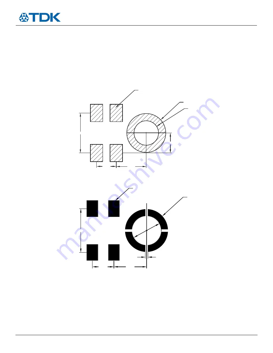
The recommended PCB land pattern for the T3903 is a 1:1 ratio of the solder pads on the microphone package, as shown in Figure 15.
Avoid applying solder paste to the sound hole in the PCB. A suggested solder paste stencil pattern layout is shown in Figure 16.
The response of the T3903 is not affected by the PCB hole size as long as the hole is not smaller than the sound port of the
microphone (0.375 mm in diameter). A 0.5 mm to 1 mm diameter for the hole is recommended. Take care to align the hole in the
microphone package with the hole in the PCB. The exact degree of the alignment does not affect the microphone performance as long
as the holes are not partially or completely blocked.
Figure 15. Recommended PCB Land Pattern Layout
Figure 16. Suggested Solder Paste Stencil Pattern Layout
PCB MATERIAL AND THICKNESS
The performance of the T3903 is not affected by PCB thickness. The T3903 can be mounted on either a rigid or flexible PCB. A
flexible PCB with the microphone can be attached directly to the device housing with an adhesive layer. This mounting method
offers a reliable seal around the sound port while providing the shortest acoustic path for good sound quality.
Ø1.025
Ø1.625
0.522x0.725(4X)
1.252
0.822
1.675
0.838
1.252
0.822
1.675
0.1(4x)
Ø1.125
Ø1.625
0.422x0.625(4X)


