background image

BIOS User's Manual

4-14

BIOS

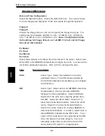
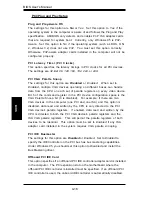
Advanced SMI Enable Controls

Timer Overflow Enable

This allows the system to generate a System Management Interrupt after

a specific amount of time has passed.  The settings are 

Enabled 

and

Disabled

.

Thermal SMI Enable

This allows the system to generate a System Management Interrupt after a

specific temperature has been exeeded.  The settings are 

Enabled 

and

Disabled

.

PME SMI Enable

This allows the system to generate a System Management Interrupt after a

Power Management Event has occurred.  The settings are 

Enabled 

and

Disabled

.

SW SMI Timer Enable

The settings for this option are 

Enabled 

and

 Disabled

.

TCO Logic SMI Enable

This allows the TCO logic to generate a System Management Interrupt when

a century rollover occurs.  The settings are 

Enabled 

and

 Disabled

.

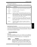
Advanced Resume Event Controls

RTC Resume

You can have the system resume operation at a predetermined time by use

of the real-time clock.  Enabling this setting allows you to determine the

following four settings.  The settings are 

Enabled 

and

 Disabled

.

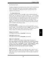
RTC Alarm Date

This allows you to set a time at which the system will wake-up.  The setting

is a number representing the alarm date.

RTC Alarm Hour

This allows you to set a time at which the system will wake-up.  The setting

is a number representing the alarm hour.

RTC Alarm Minute

This allows you to set a time at which the system will wake-up.  The setting

is a number representing the alarm minute.

Содержание Super 370SEA

Страница 1: ... SUPER 370SED SUPER 370SEA USER S MANUAL Revision 1 2 SUPER ...

Страница 2: ...machine without prior written consent IN NO EVENT WILL SUPERMICRO COMPUTER BE LIABLE FOR DIRECT INDIRECT SPECIAL INCIDENTAL OR CONSEQUENTIAL DAMAGES ARISING FROM THE USE OR INABILITY TO USE THIS PRODUCT OR DOCUMENTATION EVEN IF ADVISED OF THE POSSIBILITY OF SUCH DAMAGES IN PARTICULAR THE VENDOR SHALL NOT HAVE LIABILITY FOR ANY HARDWARE SOFTWARE OR DATA STORED OR USED WITH THE PRODUCT INCLUDING THE...

Страница 3: ...ive devices Read this chapter when you want to install the processor and DIMM memory mod ules and when mounting the mainboard in the chassis Also refer to this chapter to connect the floppy and hard disk drives the IDE interfaces the parallel and serial ports and the twisted wires for the power supply the reset button the keylock power LED the speaker and the keyboard If you encounter any problems...

Страница 4: ...iv SUPER 370SED 370SEA User s Manual Notes ...

Страница 5: ...t System Block Diagram 1 10 Motherboard Features 1 11 1 2 Chipset Overview 1 13 1 3 PC Health Monitoring 1 14 1 4 ACPI PC 98 Features 1 16 1 5 Power Supply 1 18 1 6 Super I O 1 19 Chapter 2 Installation 2 1 Static Sensitive Devices 2 1 Precautions 2 1 Unpacking 2 1 2 2 Processor Installation 2 2 2 3 Mounting the Motherboard in the Chassis 2 3 2 4 Installing DIMMs 2 4 2 5 Port Control Panel Connect...

Страница 6: ...ve Connections 2 12 Parallel Port Connector 2 13 Floppy Connector 2 13 IDE Connectors 2 13 AMR Connector 2 14 2 9 Installing Software Drivers 2 15 Chapter 3 Troubleshooting 3 1 Troubleshooting Procedures 3 1 Before Power On 3 1 No Power 3 1 No Video 3 1 Memory Errors 3 2 Losing the System s Setup Configuration 3 2 3 2 Technical Support Procedures 3 2 3 3 Frequently Asked Questions 3 3 3 4 Returnin...

Страница 7: ...e User Supervisor Password 4 21 Change Language Setting 4 22 Auto Configuration with Optimal Settings 4 22 Auto Configuration with Fail Safe Settings 4 22 Save Settings and Exit 4 22 Exit Without Saving 4 22 Appendices Appendix A BIOS Error Beep Codes and Messages A 1 Appendix B AMIBIOS Post Diagnostic Error Messages B 1 vii ...

Страница 8: ...Notes SUPER 370SED 370SEA User s Manual ...

Страница 9: ...e highest standards in quality and performance Please check that the following items have all been included with your motherboard If anything listed here is damaged or missing contact your retailer One 1 Supermicro Mainboard One 1 ATA66 ribbon cable for IDE devices One 1 Floppy ribbon cable for floppy drives One 1 Supermicro CD containing drivers and utilities One 1 5 cm heat sink fan retail packa...

Страница 10: ... CA 95131 U S A Tel 1 408 895 2001 Fax 1 408 895 2008 E mail marketing supermicro com General Information support supermicro com Technical Support Web site www supermicro com European Office Address Super Micro Computer B V Het Sterrenbeeld 28 5215 ML s Hertogenbosch The Netherlands Tel 31 0 73 6400390 Fax 31 0 73 6416525 E mail sales supermicro nl ...

Страница 11: ...Chapter 1 Introduction 1 3 Introduction Notes ...

Страница 12: ...SUPER 370SED 370SEA User s Manual 1 4 Introduction SUPER 370SED Figure 1 1 SUPER 370SED Motherboard Image ...

Страница 13: ...Chapter 1 Introduction 1 5 Introduction SUPER 370SEA Figure 1 2 SUPER 370SEA Motherboard Image ...

Страница 14: ...2 PCI 3 JF1 JF2 IR CON PW_ON RESET IDE LED KEYLOCK SPEAKER JP26 J19 FLOPPY IDE2 IDE1 1 1 J18 FAN2 Chassis Fan 1 WOL FAN3 ICH GMCH J35 Parallel Port 1 J28 7 15 J1 J9 BATTERY FAN2 JPWAKE 1 1 1 LINE OUT LINE IN MIC CD_1 CD 1 1 1 9 6 1 AMR JBT1 1 BIOS 1 Celeron Processor PPGA Package J4 VGA GAME PORT FAN3 Thermal Control Fan FAN1 CPU Fan 1 JP28 JP11 1 TV OUT JP7 1 AC 97 Audio CODEC chip 1 JL1 JP12 1 ...

Страница 15: ...nector p 2 8 COM2 COM2 Serial Port Header p 2 8 FAN1 CPU Fan Header p 2 8 FAN2 Chassis Fan Header p 2 8 FAN3 Thermal Control Fan Header p 2 8 GAME Game Port J18 J19 IDE Hard Disk Drive Connectors p 2 13 J29 ATX Power Connector p 2 6 J30 PS 2 Keyboard lower Mouse upper p 2 7 J32 J33 Universal Serial Bus Ports p 2 8 J35 Parallel Printer Port p 2 13 JF1 JF2 Front Control Panel p 2 5 JOH Overheat LED ...

Страница 16: ...YLOCK SPEAKER JP26 J19 FLOPPY IDE2 IDE1 1 1 J18 FAN2 Chassis Fan 1 WOL FAN3 ICH GMCH J35 Parallel Port 1 J28 J1 J9 BATTERY JPWAKE 1 1 1 LINE OUT LINE IN MIC CD_1 D I S P L A Y CACHE CD 1 1 1 AMR JBT1 1 BIOS D I S P L A Y CACHE J6 F PANEL GAME PORT FAN3 Thermal Control Fan FAN1 CPU Fan 1 J16 PCI 6 1 PCI 1 PCI 2 SUPER I O MONO JL1 1 JOH 1 JP28 1 FAN2 FAN1 Celeron Processor PPGA Package JP11 JP12 ISA...

Страница 17: ...rial Port Header p 2 8 FAN1 CPU Fan Header p 2 8 FAN2 Chassis Fan Header p 2 8 FAN3 Thermal Control Fan Header p 2 8 GAME Game Port J6 Direct Digital Flat Panel Connector p J18 J19 IDE Hard Disk Drive Connectors p 2 13 J29 ATX Power Connector p 2 6 J30 PS 2 Keyboard lower Mouse upper p 2 7 J32 J33 Universal Serial Bus Ports p 2 8 J35 Parallel Printer Port p 2 13 JF1 JF2 Front Control Panel p 2 5 J...

Страница 18: ...241 BGA SDRAM 133 100 66 MHz Host Bus PCI Slots USB ATA66 IDE Ports BIOS 4Mb FWH 4MB Display Cache 33 MHz PCI Bus 100 MHz SDRAM Bus SuperI O LPC 1 5 Mb sec AC 97 AMR 133 100 MHz Bus Note This is a general block diagram and may not represent the actual number of PCI ISA slots on your motherboard See the following page for the actual specifications of each motherboard ...

Страница 19: ... speed being used Chipset Intel 810E 82810E GMCH w 4 MB display cache 82801AA ICH see page 1 13 for details Expansion Slots 370SED 370SEA 3 PCI slots 6 PCI slots 1 ISA slots 1 PCI ISA slot shared 1 AMR slot 1 AMR slot BIOS 4 Mb Firmware Hub AMI Flash BIOS APM 1 2 DMI 2 1 PCI with PME support ACPI 1 0 Plug and Play PnP PC Health Monitoring Seven onboard voltage monitors for CPU core chipset voltage...

Страница 20: ...and PS 2 keyboard ports 1 infrared port slow IR 2 USB Universal Serial Bus ports TV Out header 370SED only Direct Digital Flat Panel Connector 370SEA only Other Selectable CPU speed control set in BIOS Keyboard wake up Internal external modem ring on AC 97 2 1 compliant link for audio and telephony CODECs Onboard Direct AGP graphics controller with D V M T and 4 MB display cache see GMCH on page 1...

Страница 21: ...between the SDRAM and the rest of the system logic It includes a system memory DRAM controller which supports a 64 bit 100 MHz DRAM array and utilizes Direct AGP integrated AGP technology to create vivid 2D and 3D effects and images Direct AGP features D V M T Dynamic Video Memory Tech nology which provides richer graphics by dynamically utilizing memory to meet changing graphic demands efficientl...

Страница 22: ...running ACPI for this feature to take effect See page 1 16 for details on initiating ACPI All drivers and add on cards must be ACPI supported for STR to function Recovery from AC Power Loss BIOS provides a setting for you to determine how the system will respond when AC power is lost and then restored to the system You can choose for the system to remain powered off in which case you must hit the ...

Страница 23: ... the CPU The onboard chassis thermal circuitry can monitor the overall system temperature and alert users when the chassis temperature is too high CPU Fan Auto Off in Sleep Mode The CPU fan activates when the power is turned on It can be turned off when the CPU is in sleep mode When in sleep mode the CPU will not run at full power thereby generating less heat CPU Overheat LED and Control This feat...

Страница 24: ...cally turn on and off peripherals such as CD ROMs network cards hard disk drives and printers This also includes consumer devices connected to the PC such as VCRs TVs tele phones and stereos In addition to enabling operating system directed power management ACPI provides a generic system event mechanism for Plug and Play and an oper ating system independent interface for configuration control ACPI...

Страница 25: ...on as a system suspend button When the user depresses the power button the system will enter a SoftOff state The monitor will be suspended and the hard drive will spin down Depressing the power button again will cause the whole system to wake up During the SoftOff state the ATX power supply provides power to keep the required circuitry in the system alive In case the system malfunctions and you wa...

Страница 26: ...PU clock rates of 300 MHz and above The SUPER 370SED 370SEA accommodates ATX power supplies Although most power supplies generally meet the specifications required by the CPU some are inadequate It is strongly recommended that you use a high quality power supply that meets ATX power supply Specification 2 01 or above Additionally in areas where noisy power transmission is present you may choose to...

Страница 27: ... rates of 250 Kb s 500 Kb s or 1 Mb s It also provides two high speed 16550 compatible serial communication ports UARTs one of which supports serial infrared communication Each UART includes a 16 byte send receive FIFO a programmable baud rate generator complete modem control capability and a processor interrupt sys tem Both UARTs provide legacy speed with baud rate of up to 115 2 Kbps as well as ...

Страница 28: ...SUPER 370SED 370SEA User s Manual 1 20 Introduction Notes ...

Страница 29: ...tal object before removing the board from the antistatic bag Handle the board by its edges only do not touch its components peripheral chips memory modules or gold contacts When handling chips or modules avoid touching their pins Put the motherboard and peripherals back into their antistatic bags when not in use For grounding purposes make sure your computer chassis provides excellent conductivity...

Страница 30: ...ched corner of the processor oriented with pin 1 Fully seat the processor into the socket and then close the lever See Figure 2 1 for views of the PPGA 370 pin socket before and after processor instal lation 2 2 Processor Installation When handling the processor package avoid placing direct pressure on the label area of the fan The following pages cover the installation procedure You should instal...

Страница 31: ...include a variety of mounting fasteners made of metal or plastic Although a chassis may have both types metal fasteners are the most highly recommended because they ground the motherboard to the chassis For this reason it is best to use as many metal fasteners as possible Pin 1 Lever Processor installed Notched Corner Figure 2 1 PPGA Socket Empty and with Processor Installed ...

Страница 32: ... Insert DIMMs in Bank 0 through Bank 1 as required for the desired system memory 2 Insert each DIMM module vertically into its slot Pay attention to the two notches along the bottom of the module to prevent inserting the DIMM incorrectly 3 Gently press down on the DIMM module until it snaps into place in the slot 4 If installing only a single DIMM you may use either Bank 0 or 1 To Remove Use your ...

Страница 33: ...ous I O ports Note The port layout is different for each board Parallel Port Burgundy Game Port Gold COM1 Port Turquoise Keyboard Purple Mouse Green USB Ports Black Figure 2 3 I O Port Locations and Definitions VGA Monitor Port Blue Mouse Green Keyboard Purple USB Ports Black Flat Panel Port Black VGA Monitor Port Blue Parallel Port Burgundy Game Port Gold Line Out Line In Mic Lime Light blue Pink...

Страница 34: ...rs See Figure 2 4 for the pin definitions of the speaker keyboard lock hard drive LED infrared connector and power on and reset button headers which are all located on JF1 and JF2 Refer to pages 2 7 to 2 8 for details Speaker IR Conn Power On X Reset JF2 JF1 X Keyboard Lock 1 1 Hard Drive LED Power LED Figure 2 4 Front Control Panel Connectors ...

Страница 35: ...ve securely mounted the motherboard memory and add on cards you are ready to connect the cables Attach an ATX power supply cable to J29 by aligning the tabs on both connectors See Table 2 1 for the pin definitions of an ATX power supply Table 2 1 ATX Power Supply Connector Pin Definitions J29 Pin Number Definition 1 3 3V 2 3 3V3 3 Ground 4 5V 5 Ground 6 5V 7 Ground 8 PW OK 9 5VSB 10 12V Pin Number...

Страница 36: ... 5 for pin definitions Speaker Connector The speaker connector is located on pins 10 to 13 of JF1 See Table 2 7 for pin definitions Table 2 7 Speaker Connector Pin Definitions JF1 Pin Number 10 11 12 13 Function Key Definition Red wire Speaker data No connection Key Speaker data ATX PS 2 Keyboard and PS 2 Mouse Ports The ATX PS 2 keyboard and the PS 2 mouse are located on J30 See Table 2 8 for pin...

Страница 37: ... fan headers are located on FAN1 and FAN2 respectively Refer to Table 2 12 for pin definitions Universal Serial Bus USB The two Universal Serial Bus con nectors are located on J32 and J33 See Table 2 9 for pin definitions Table 2 9 Universal Serial Bus Pin Definitions Pin Number Definition 1 5V 2 P0 3 P0 4 Ground 5 N A Pin Number Definition 1 5V 2 P0 3 P0 4 Ground 5 Key J32 J33 Serial Ports The se...

Страница 38: ... pin definitions Pin Number 1 2 Definition 12VDC OH Active Table 2 14 Overheat LED Pin Definitions JOH Chassis Intrusion The Chassis Intrusion header is lo cated on JL1 See the board layouts in Chapter 1 for its location See Table 2 15 for pin definitions Pin Number 1 2 Definition Intrusion Input Ground Table 2 15 Chassis Intrusion Pin Definitions JL1 TV Out Header 370SED only The TV Out header al...

Страница 39: ...ging the CPU speed is en abled by software control in BIOS see CPU Speed on page 4 10 The CPU Speed setting will show you the actual CPU speed for each FSB speed option selected The FSB speed is set with JP11 and JP12 Table 2 17 displays the set tings for these two jumpers Note If the system does not reboot after changing the CPU speed 1 clear CMOS and reboot as described on next page and then set...

Страница 40: ...ed onboard and the AMR slot will support modems only The disabled setting should be se lected when you wish to use an add on card for audio either in the AMR or a PCI slot See Table 2 19 for jumper settings Jumper Position 1 2 2 3 Definition Enabled Disabled Table 2 19 AC 97 Enable Disable Jumper Settings JP28 CMOS Clear Refer to Table 2 18 for instruc tions on how to clear CMOS Al ways remove the...

Страница 41: ...ors to support two drives This special cable should be used to take advantage of the speed this new technology offers The blue connector connects to the onboard IDE connector interface and the other connector s to your hard drive s Consult the documentation that came with your disk drive for details on actual jumper locations and settings TV Out Mode 370SED only The digital PC to TV circuitry inte...

Страница 42: ...itions J35 Pin Number Function 1 GND 3 GND 5 Key 7 GND 9 GND 11 GND 13 GND 15 GND 17 GND 19 GND 21 GND 23 GND 25 GND 27 GND 29 GND 31 GND 33 GND Pin Number Function 2 FDHDIN 4 Reserved 6 FDEDIN 8 Index 10 Motor Enable 12 Drive Select B 14 Drive Select A 16 Motor Enable 18 DIR 20 STEP 22 Write Data 24 Write Gate 26 Track 00 28 Write Protect 30 Read Data 32 Side 1 Select 34 Diskette Table 2 23 Flopp...

Страница 43: ...B9 B10 B11 B12 B13 B14 B15 B16 B17 B18 B19 B20 B21 B22 B23 Signal AUDIO_PWRDN MONO_PHONE GND 5Vdual 5VSB USB_OC GND USB USB KEY KEY GND S P DIF_IN GND 3 3Vdual 3 3VSB GND AC97_SYNC GND AC97_SDATA_IN1 GND AC97_SDATA_IN0 GND AC97_BITCLK Pin Number A1 A2 A3 A4 A5 A6 A7 A8 A9 A10 A11 A12 A13 A14 A15 A16 A17 A18 A19 A20 A21 A22 A23 Table 2 25 AMR Connector Pin Definitions AMR AMR Connector Refer to Tab...

Страница 44: ...XC 7 GND 8 5V 9 10 11 TX2 12 TX2 13 SHLD2 14 SHLD0 15 TX0 16 TX0 17 18 HPD 19 DDC_DAT 20 DDC_CLK Description TMDS Pos Diff Out Ch1 TMDS Neg Diff Out Ch1 Shield for TMDS Ch1 Shield for TMDS clock TMDS Pos Diff Out Ref Clk TMDS Neg Diff Out Ref Clk Logic Ground Logic 5V Supply No Connection No Connection TMDS Pos Diff Out Ch2 TMDS Neg Diff Out Ch2 Shield for TMDS Ch2 Shield for TMDS Ch0 TMDS Pos Dif...

Страница 45: ...n Click the icons showing a hand writing on paper to view the readme files for each item Click the tabs to the right of these in order from top to bottom to install each item one at a time After installing each item you must reboot the system before moving on to the next item on the list You should install everything here except for the SUPER Doctor utility which is optional The Security and Graph...

Страница 46: ...2 18 SUPER 370SED 370SEA User s Manual Installation Notes ...

Страница 47: ...it is fully seated the chassis speaker and the power LED to the motherboard Check all jumper settings as well 5 Install a single memory module and make sure it is fully seated 6 Check the power supply voltage 115V 230V switch No Power 1 Make sure no short circuits exist between the motherboard and chassis 2 Verify that all jumpers are set to their default positions 3 Turn the power switch on and o...

Страница 48: ...y should know of any possible problem s with the specific system configuration that was sold to you 1 Please go through the Troubleshooting Procedures and Frequently Asked Question FAQ sections in this chapter or see the FAQs on our web site http www supermicro com techsupport htm before contacting Technical Support 3 Use the speaker to determine if any beep codes exist Refer to Appendix A for det...

Страница 49: ...an support Answer Your motherboard has two DIMM sockets that support 168 pin unbuffered 3 3V SDRAM It does not support registered ECC or EDO memory Note that whether running at 66 or 100 MHz FSB speed the memory must be PC100 compliant Because ECC is not supported using ECC memory will result in non ECC operation Question How do I update my BIOS Answer It is recommended that you do not upgrade you...

Страница 50: ...e at the same time then turn on the power with these keys pressed until your floppy drive starts reading Your screen will remain blank until the BIOS program is done If the system reboots correctly then the recovery was successful The BIOS Recovery Procedure will not update the boot block in your BIOS Question Do I need the CD that came with your motherboard Answer The supplied compact disc has qu...

Страница 51: ... connect the ATA66 cable to my IDE device s Answer The 80 wire 40 pin ATA66 IDE cable that came with your system has two connectors to support two drives This special cable must be used to take advantage of the speed the ATA66 technology offers Con nect the blue connector to the onboard IDE header and the other connector s to your hard drive s Consult the documentation that came with your disk dri...

Страница 52: ...System Management bus Question Where can I get a driver to use DVD with the TV Out function Answer A DVD driver that we recommend can be downloaded from http www cyberlink com tw english products powerdvd htm This also applies to using DVD with a monitor We also expect to soon have DVD driver information posted on our web site Question I see some of my PCI devices sharing IRQs but the sys tem seem...

Страница 53: ...rning to the manufacturer the RMA number should be prominently displayed on the outside of the shipping carton and mailed prepaid or hand carried Ship ping and handling charges will be applied for all orders that must be mailed when service is complete This warranty only covers normal consumer use and does not cover damages incurred in shipping or from failure due to the alternation misuse abuse o...

Страница 54: ...3 8 SUPER 370SED 370SEA User s Manual Troubleshooting Notes ...

Страница 55: ...when the computer is turned off The original IBM AT had 64 kbytes of non volatile memory storage in CMOS RAM All AT compatible systems have at least 64 kbytes of CMOS RAM which is usually part of the Real Time Clock Many systems have 128 kbytes of CMOS RAM How Data Is Configured AMIBIOS provides a Setup utility in ROM that is accessed by pressing Del at the appropriate time during system boot Setu...

Страница 56: ...toring chips When a failure occurs in a monitored activity AMIBIOS can sound an alarm and display a message The PC Health Monitoring chips monitor CPU temperature Additional temperature sensors Chassis intrusion detector Five positive voltage inputs Two negative voltage inputs Three fan speed monitor inputs 4 3 Running Setup Optimal default settings are in bold text unless otherwise noted The BIOS...

Страница 57: ...Sector Virus Protection Disabled Month Jan Dec ESC Exit Sel Day 01 31 PgUp PgDn Modify Year 1901 2099 F2 F3 Color AMIBIOS HIFLEX SETUP UTILITY VERSION 1 18 1998 American Megatrends Inc All Rights Reserved STANDARD CMOS SETUP ADVANCED CMOS SETUP ADVANCED CHIPSET SETUP POWER MANAGEMENT SETUP PCI PLUG AND PLAY SETUP PERIPHERAL SETUP AUTO DETECT HARD DISK CHANGE USER PASSWORD CHANGE SUPERVISOR PASSWOR...

Страница 58: ...with a list of drive parameters appears Click on OK to configure the drive Type How to Configure SCSI Select Type Select Not Installed on the drive parameter screen The SCSI drivers provided by the SCSI manufacturer should allow you to configure the SCSI drive IDE Select Type Select Auto to let AMIBIOS determine the parameters Click on OK when AMIBIOS displays the drive parameters Select LBA Mode ...

Страница 59: ... per track SCSI and IDE drive may have even more sectors per track Capacity The formatted capacity of the drive is Number of heads x Number of cylinders x Number of sectors per track x 512 bytes per sector Boot Sector Virus Protection This setting allows you to prevent any data from being written the boot sector of the hard drive While this may prevent viruses from infecting your system you may ne...

Страница 60: ...The options for the 1st Boot Device are Disabled 1st IDE HDD 2nd IDE HDD 3rd IDE HDD 4th IDE HDD Floppy ARMD FDD ARMD HDD ATAPI CD ROM SCSI Network or I2 0 The options for the 2nd Boot Device are Disabled 1st IDE HDD 2nd IDE HDD 3rd IDE HDD 4th IDE HDD Floppy ARMD FDD ARMD HDD ATAPI CD ROM or SCSI The options for the 3rd Boot Device are Disabled 1st IDE HDD 2nd IDE HDD 3rd IDE HDD 4th IDE HDD Flop...

Страница 61: ...een Floppy Access Control The settings for this option are Read Write or Read Only Hard Disk Access Control The settings for this option are Read Write or Read Only S M A R T for Hard Disks S M A R T Self Monitoring Analysis and Reporting Technology is a technology developed to manage the reliability of the hard disk by predicting future device failures The hard disk needs to be S M A R T capable ...

Страница 62: ...or this option are Disabled WriteThru or WriteBack System BIOS Cacheable When set to Enabled the contents of the F0000h system memory segment can be read from or written to cache memory The contents of this memory segment are always copied from the BIOS ROM to system RAM for faster execution The settings are Enabled or Disabled Note The Optimal default setting is Enabled and the Fail Safe default ...

Страница 63: ...the USB Universal Serial Bus functions USB KB Mouse Legacy Support The settings for this option are Keyboard Auto Keyboard Mouse or Dis abled Set this option to Enabled to enable the USB keyboard and mouse CPU Latency Timer See details on setup secreen The settings for this option are Enabled and Disabled Dram Page Closing See details on setup secreen The settings for this option are Open and Clos...

Страница 64: ...indow Size This option specifies the cache size to be used for the display data The settings are 32MB and 64MB CPU Speed at 133 100 66 MHz This option allows you to change the CPU speed unless Auto has been selected with JP 11 and 12 The Reserved settings will cause no change The other settings list the CPU speeds the paired numbers list the CPU speed at 133 100 and 66 MHz FSB respectively The fir...

Страница 65: ...this option are Enabled or Disabled AC97 Modem Controller This setting is used to switch between use of the Audio Modem Riser AMR and a modem The settings for this option are Auto or Disabled AC97 Audio Controller This setting is used to switch the onboard audio on and off The settings for this option are Auto or Disabled SMBus Controller The settings for this option are Enabled and Disabled DMA0 ...

Страница 66: ...n this section only You may be able to toggle between settings on the other options but it will have no effect Standby Time Out This option specifies the length of a period of system inactivity while in the full power on state When this length of time expires the computer enters a standby power state The settings are Disabled 1Min 5Min and 10Min Suspend Power Saving Type The settings for this opti...

Страница 67: ...of hard drive inactivity has expired The settings are Disabled Standby or Suspend Note The Optimal default setting for this option is Suspend and the Fail Safe default setting is Disabled Hard Disk Time Out Minutes This option specifies the length of a period of hard disk drive inactivity When this length of time expires the computer enters the power conserving state specified in the Hard Disk Pow...

Страница 68: ...ed and Disabled TCO Logic SMI Enable This allows the TCO logic to generate a System Management Interrupt when a century rollover occurs The settings are Enabled and Disabled Advanced Resume Event Controls RTC Resume You can have the system resume operation at a predetermined time by use of the real time clock Enabling this setting allows you to determine the following four settings The settings ar...

Страница 69: ... settings for this option are Enabled and Disabled SM BUS Resume This allows you to wake up the system from a system management bus device The settings for this option are Enabled and Disabled LAN Wake Up This allows you to make use of the Wake on LAN feature The settings for this option are Enabled and Disabled Suspend to RAM Support This allows you to Enable or Disable the Suspend to RAM feature...

Страница 70: ... register in the PCI device configuration space is the VGA Palette Snoop bit 0 is disabled For example if there are two VGA devices in the computer one PCI and one ISA and this option is disabled data read and written by the CPU is only directed to the PCI VGA device s palette registers If enabled data read and written by the CPU is directed to both the PCI VGA device s palette registers and the I...

Страница 71: ...IRQ These options specify the PCI interrupt used by the primary or secondary IDE channel on the offboard PCI IDE controller The settings are Disabled Hardwired INTA INTB INTC or INTD PCI Slot1 IRQ Priority PCI Slot2 IRQ Priority PCI Slot3 IRQ Priority PCI Slot4 IRQ Priority Use these options to specify the IRQ priority for PCI devices installed in the PCI expansion slots The settings are Auto IRQ ...

Страница 72: ...ared IRQs Reserved Memory Size This option specifies the size of the memory area reserved for legacy ISA adapter cards The settings are Disabled 16K 32K or 64K Reserved Memory Address This option specifies the beginning address in hex of the reserved memory area The specified ROM memory area is reserved for use by legacy ISA adapter cards The settings are C0000 C4000 C8000 CC000 D0000 D4000 D8000 ...

Страница 73: ...us monitor Onboard FDC This option enables the FDC Floppy Drive Controller on the motherboard The settings are Disabled and Enabled Onboard Serial Port 1 This option specifies the base I O port address of serial port 1 The settings are Disabled 3F8h 2F8h 3E8h and 2E8h Onboard Serial Port 2 This option specifies the base I O port address of serial port 2 The settings are Disabled 3F8h 2F8h 3E8h and...

Страница 74: ...mal default setting for this option is ECP and the Fail Safe setting is Normal EPP Version The settings are 1 7 and 1 9 Note The Optimal and Fail Safe default settings are N A Parallel Port IRQ This option specifies the IRQ to be used by the parallel port The settings are 5 and 7 Parallel Port DMA Channel This option is only available if the setting of the parallel port mode op tion is ECP The set...

Страница 75: ...l users must enter a password every time the system boots or when the AMIBIOS setup is executed You can set either a Supervisor password or a User password If you do not want to use a password just press Enter when the password prompt appears The password check option is enabled in the Advanced Setup by choosing either Always or Setup The password is stored in CMOS RAM You can enter a password by ...

Страница 76: ...uto Configuration with Fail Safe Settings The Fail Safe default settings consist of the safest set of parameters Use them if the system is behaving erratically They should always work but do not provide optimal system performance characteristics Save Settings and Exit Highlight this and hit Enter when you wish to save any changes made to settings in BIOS and exit back to the system boot up procedu...

Страница 77: ...the screen Fatal errors are those which will not allow the system to continue the boot up procedure If a fatal error occurs you should consult with your system manufacturer for possible repairs These fatal errors are usually communicated through a series of audible beeps The numbers on the fatal error list on the following page correspond to the number of beeps for the corresponding error All erro...

Страница 78: ...the CPU into protected mode Reseat or replace the 8042 chip try another keyboard or check keyboard fuse if present 7 No flash present No flash part detected The BIOS cannot be updated 8 The ROM checksum value Error reported in ROM checksum does not match the value BIOS chip most likey needs replaced encoded in the BIOS 9 The system video adapter is Absent or faulty video adapter detected either mi...

Страница 79: ...er Replace the video adapter or the RAM on the video adapter 13 times there is a ROM checksum error This usually means the BIOS chip needs replaced If you hear it s because 5 short and 1 long beeps EDO memory detected in system 6 short and 1 long beeps Reg or BUFF SDRAM detected in system 7 short and 1 long beeps 4M SDRAM detected in system 8 short and 1 long beeps 12M SDRAM detected in system 9 s...

Страница 80: ...H 2 Timer Error Most ISA computers include two times There is an error in time 2 CMOS Battery State Low CMOS RAM is powered by a battery The battery power is low Replace the battery CMOS Checksum Failure After CMOS RAM values are saved a checksum value is generated for error checking The previous value is different from the current value Run WINBIOS Setup or AMIBIOS Setup CMOS System Option The va...

Страница 81: ...k and follow the screen instructions Display Switch Some compters require a video switch on the Not Proper motherboard be set to either color or monochrome Turn the computer off set the switch then power on DMA Error Error in the DMA controller DMA 1 Error Error in the first DMA channel DMA 2 Error Error in the second DMA channel FDD Controller Failure The BIOS cannot communicate with the floppy d...

Страница 82: ...or No ROM BASIC Cannot find a bootable sector on either disk drive A or hard disk drive C The BIOS calls INT 18h which generates this message Use a bootable disk Off Board Parity error in memory installed in an Parity Error expansion slot The format is OFF BOARD PARITY ERROR ADDR HEX XXXX XXXX is the hex address where the error occurred Run AMIDiag to find and correct memory problems On Board Pari...

Страница 83: ...disabling cache memory 06 Uncompressing the post code unit next 07 Next initializing the CPU init and the CPU data area 08 The CMOS checksum calculation is done next 0B Next performing any required initialization before keyboard BAT command is issued 0C The keyboard controller I B is free Next issuing the BAT command to the keyboard controller 0E The keyboard controller BAT command result has been...

Страница 84: ...chipset 14 The 8254 timer test will begin next 19 The 8254 timer test is over Starting the memory refresh test next 1A The memory refresh test line is toggling Checking the 15 second on off time next 23 Reading the 8042 input port and disabling the MEGAKEY Green PC feature next Making the BIOS code segment writable and performing any necessary configuration before initializing the interrupt vector...

Страница 85: ...d control to BIOS POST Performing any required processing after the video ROM had control 2E Completed post video ROM test processing If the EGA VGA controller is not found performing the display memory read write test next 2F The EGA VGA controller was not found The display memory read write test is about to begin 30 The display memory read write test passed Look for retrace checking next 31 The ...

Страница 86: ... at 0 0 next 45 Data initialized Checking for memory wraparound at 0 0 and finding the total system memory size next 46 The memory wraparound test has completed The memory size calculation has been completed Writing patterns to test memory next 47 The memory pattern has been written to extended memory Writing patterns to the base 640 KB memory next 48 Patterns written in base memory Determining th...

Страница 87: ...ized Adjusting the displayed memory size for relocation and shadowing next 51 The memory size display was adjusted for relocation and shadowing Testing the memory above 1 MB next 52 The memory above 1 MB has been tested and initialized Saving the memory size information next 53 The memory size information and the CPU registers are saved Entering real mode next 54 Shutdown was successful The CPU is...

Страница 88: ...aring the output buffer and checking for stuck keys Issuing the keyboard reset command next 81 A keyboard reset error or stuck key was found Issuing the keyboard controller interface test command next 82 The keyboard controller interface test completed Writing the command byte and initializing the circular buffer next 83 The command byte was written and global data initialization has been complete...

Страница 89: ...e PS 2 mouse check and extended BIOS data area allocation check next 8C Programming the WINBIOS Setup options next 8D The WINBIOS Setup options are programmed Resetting the hard disk controller next 8F The hard disk controller has been reset Configuring the floppy drive controller next 91 The floppy drive controller has been configured Configuring the hard disk drive controller next 95 Initializin...

Страница 90: ...d initialization after the Coprocessor test next 9E Initialization after the Coprocessor test is complete Checking the extended keyboard keyboard ID and Num Lock key next Issuing the keyboard ID command next A2 Displaying any soft errors next A3 The soft error display has completed Setting the keyboard typematic rate next A4 The keyboard typematic rate is set Programming the memory wait states nex...

Страница 91: ... DMI B1 Copying any code to specific areas D0h The NMI is disabled Power on delay is starting Next the initialization cade checksum will be verified D1h Initializing the DMA controller Performing the keyboard controller BAT test Starting memory refresh and entering 4 GB flat mode next D3h Starting memory sizing next D4h Returning to real mode Executing any OEM patches and setting the stack next D5...

Страница 92: ...BIOS User s Manual B 10 APPENDIX B If either Ctrl Home was pressed or the system BIOS checksum is bad next the system will go to checkpoint code E0h Otherwise going to checkpoint code D7h ...

Отзывы: