Pin
number
Description
Assignment
Pin
number
Description
Assignment
13
TX
T_VCP_RX (PC11)
14
RX
T_VCP_TX (PC10)
Note:
4-wire and 5-wire JTAG Debug modes are not supported by default. 4-wire JTAG mode may be used, but may
require to deactivate USB Type-C
®
feature in hardware and software, to connect JTDI with the SB28 solder
bridge and to disconnect R89.
14.2.2
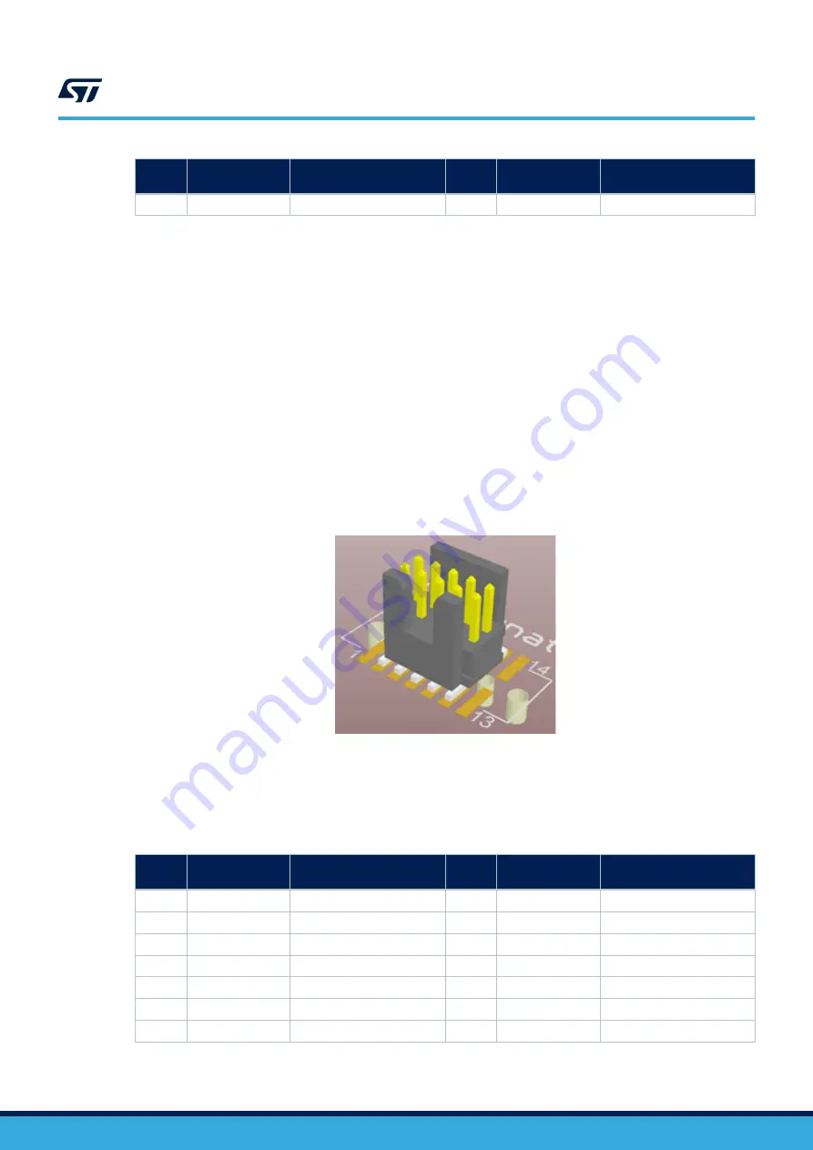
CN1 MIPI10 debug connector
The MIPI10 debug connector is implemented to program and debug the STM32G474RET6 microcontroller. The
SWD protocol must be used by default.
To use the MIPI10 connector to debug STM32G474RET6, it is mandatory to place a jumper on JP6 to connect
STLK NRST to GND. This sets the STLINK-V3E MCU in the high-impedance state.
In case the user wants to completely isolate the MIPI10 debug connector from STLINK-V3E MCU, SW1 octal
mechanical switch must be set accordingly, and JP7 must be removed. This also disconnects the
STM32G474RET6 microcontroller from STLINK-V3E.
The MIPI10 male connector is soldered on the STDC14 footprint. Pin 1 of MIPI10 is connected to pin 3 of
STDC14 footprint.
Figure 23.
CN1 MIPI10 debug connector
With onboard MIPI10 connector, the T_VCP_RX (PC11) and T_VCP_TX (PC10) signals remain easily accessible
on the CN9 extension connector.
Table 15.
MIPI10 on STDC14 footprint
Pin
number
Description
Assignment
Pin
number
Description
Assignment
1
-
-
2
-
-
3
3V3 power
3V3
4
SWDIO / JTMS
T_SWDIO (PA13)
5
GND
GND
6
SWCLK / JTCK
T_SWCLK (PA14)
7
KEY
GND
8
SWO / JTDO
T_SWO (PB3)
9
-
-
10
JTDI
T_JTDI (PA15)
11
GNDDetect
100 Ω pull-down
12
RESET / JTRST
T_NRST (PG10)
13
TX
T_VCP_RX (PC11)
14
RX
T_VCP_TX (PC10)
UM2577
CN1 debug connector
UM2577
-
Rev 2
page 35/54


