- 57 -
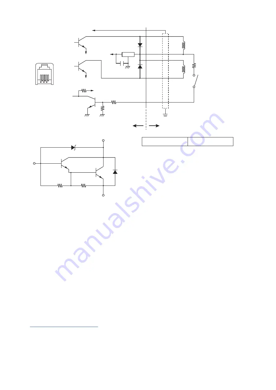
Drive circuit
Handling Precautions
1) Peripheral devices 1 and 2 cannot be driven simultaneously.
2) To continuously drive the peripheral device, keep the duty cycle less than or equal to 20%.
3) If you connect a cash drawer or similar device, be sure not to set bit 2 of memory switch #7 to 1. Doing so may damage the
connected device and the drive circuit.
4) You can use the status command to query the compulsion switch state.*
5) Minimum resistance for coils L1 and L2 is 24 Ω.
6) Absolute maximum rating of diodes D1 and D2 (Ta = 25°C)
Average rectified current I
o
= 1.0 A
7) Absolute maximum rating for transistors TR1 and TR2 (Ta = 25°C)
Collector current I
C
= 2.0 A
* For details of commands, see the separate Programmer’s Manual.
http://www.star-m.jp/eng/dl/dl02.htm
Drive output
24 V, 1.0 A max.
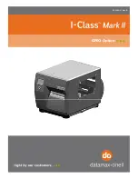
Reference
2SD 1866 Circuit Diagram
TR1, 2: 2SD 1866 or equivalent
R1 = 10 k
Ω
R2 = 33 k
Ω
6 1
1
2
3
4
5
6
F.G
D1
D2
TR1
TR2
TR3
R2
+24V
7824
R1
Vcc
R3
4.7K
Ω
1/4W
M-GND
M-GND
L1
L2
E
C
R3
R4
R3= 3.5K
Ω
R4= 300
Ω
B
With shield
Peripheral device 1
Peripheral
device 2
Compulsion switch
Frame ground
Printer side
User side
6-pin modular
jack connector
Содержание FVP10 SERIES
Страница 1: ...THERMAL PRINTER FVP10 SERIES Hardware Manual ...
Страница 67: ...URL http www star m jp eng ...


