background image

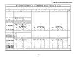
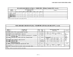
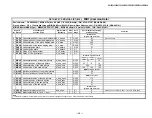
KV-32HS20/36HS20/36HS20H/32XBR450/36XBR450/36XBR450H

— 27 —

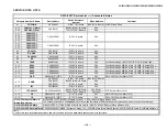
UHF
VHF

CV

SV

YPbPr

480i

YPbPr

480p

YPbPr

1080i

P&P

0

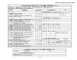
SYSM

 SYSTEM: Signal bandwidth setting

0~3

1

1

1

1

1

2

2

1

UVML

 VM_LEV: VM_OUT level

C

0~3

3

2

VMMO

 System Micro pin#40

0, 1

0

0

0

0

0

0

0

3

VMCR

 VM_COR: VM_OUT coring level

0~3

3

3

3

3

3

3

3

4

VMLM

 VM_LMT: VM_OUT limit level

0~3

3

3

3

3

3

3

3

5

VMF0

 VM_F0: VM_f0

0~3

2

2

2

2

2

2

2

6

VMDL

 VM_DLY: VM_OUT phase (defined by phase difference from R_OUT)

0~3

3

3

3

3

3

1

3

7

SHOF

 Offset for USHP = SHOF x 4

0~3

2

2

2

3

3

0

2

8

SHF0

 SHP_F0: Sharpness circuit f0

0, 1

1

1

1

1

1

0

1

9

PROV

 PRE/OVER: Y signal pre/over-shoot ratio

0~3

3

3

3

1

3

0

3

10

F1LV

 SHP_F1: Sharpness for higher f0 (4.2/5.6 MHz @ NORMAL mode)

0~3

0

3

3

3

3

3

3

11

CDSP

 SHP_CD: Sharpness in part of high color saturaion

0~3

3

3

3

3

3

3

3

12

LTLV

 LTI_LEV: Luminance transient improvement (LTI)

0~3

3

3

3

3

3

3

3

13

LTMD

 LTI_MODE: LTI mode setting

0~3

0

0

0

0

0

0

1

14

CTLV

 CTI_LEV:  Chrominance transient improvement (CTI)

0~3

0

0

0

0

0

2

0

15

CTMD

 CTI_MODE: CTI mode setting

0~3

0

0

0

0

0

0

0

16

UBOF

 Offset for UBRT (Picture clarity adjustment)

0~(7)~15

7

7

7

7

7

10

7

17

UCOF

 Offset for UCOL = UCOF x 2 (Picture clarity adjustment)

0~3

3

3

3

3

3

0

3

18

UHOF

 Offset for UHUE (Picture clarity adjustment)

0~3

0

0

0

0

0

0

0

19

MIDE

 MID enhancement setting

0~15

3

3

3

7

11

---

---

Data

Type

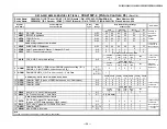
DX1A-2001&2000 SERVICE LIST (#3-3):   

CXA2150P-3  {Picture Controls: P3

}   

(Part-1/3)

Comment

Register

No & Name

 Note:

 The same CXA2150 service data are used for DX1A-2001&2000. 

Data

Range

 Device Name:     CXA2150AQ  { CRT Driver / SONY } / IC201 (A-board) / P/N: 8-752-093-35 (SBorSD#: NA)
 Slave Address:   86h

Picture Mode: Vivid

Data Initial/Average Settings 

(32V&36V CRTs)

Control Register

Function & Link

 These settings
 continue to
 the next page.

 CV:
 CVideo1~4
 SV:
 SVideo1~3

 C:
 Common data

 ( ): Settings at
       center

Содержание WEGA KV-32XBR450

Страница 1: ...LEVISION SERVICE MANUAL DX 1A CHASSIS MODEL NAME REMOTE COMMANDER DESTINATION CHASSIS NO KV 32XBR450 RM Y184 US SCC S47D A KV 32XBR450 RM Y184 CND SCC S48D A SelfDiagnosis Supported model 9 965 898 01 KV 32XBR450 RM Y184 ...

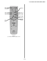
Страница 2: ... not reset properly as follows RESETTING THE DEFLECTION NVM DATA 1 Enter into service mode 2 Press 7 then MENU and then press ENTER on the remote RESETTING THE SYSTEM NVM DATA 1 Enter into service mode 2 Press 7 then 9 and then press ENTER on the remote RESETTING THE SYSTEM NVM DATA 1 Enter into service mode 2 Press 8 and then press ENTER on the remote 4 2 MEMORY WRITE CONFIRMATION METHOD 1 After ...

Страница 3: ... KV 32HS20 36HS20 36HS20H 32XBR450 36XBR450 36XBR450H RM Y184 KV 32XBR450 36XBR450 36XBR450H ONLY WRITE INTO MEMORY ITEM UP ITEM DOWN TEST RESET DEVICE UP DATA UP DATA DOWN DEVICE DOWN EXECUTE READ MEMORY ...

Страница 4: ...06V2ME 153FP IC701 A board 60h DX1A 2001 System Micro V1 0 mPD64082 IC3501 BC board B8h W B9h R CXA2103Q IC3048 Main B board 9Ah CXA2150Q IC201 A board 86h 16 ID1 CXD2085M IC3603 B board 40h IC3602 Main B board 68h Main IC3601 Sub B board 6Ch Sub 18 OP M306V2ME 153FP IC701 A board 60h DX1A 2001 System Micro V1 0 19 ID M306V2ME 153FP IC701 A board 60h DX1A 2001 System Micro V1 0 DX1A 2001 System Mi...

Страница 5: ...or Hsync non standard signal detection out of Hsync intra field 0 3 1 1 1 15 LDSR Sensitivity for frame non standard signal detection out of Hsync inter frame 0 3 2 2 2 VM Off VM Low VM Mid VM High 16 VAPG V aperture compensation gain 0 7 0 2 3 4 17 VAPI V aperture compensation convergence point 0 31 4 4 4 SNNR 0 SNNR 1 SNNR 2 SNNR 3 18 YPFT Y peaking filter BPF center frequency 0 3 0 0 0 0 0 19 Y...

Страница 6: ...tion filter characteristic 0 1 0 0 0 36 HDP Fine adjustment of the system H phase C 0 7 5 37 BGPS Internal burst gate start position Gate Start Position from Hsync center 0 25 x BGPS 2 C 0 15 4 38 BGPW Internal burst gate width Gate Width 0 25 x BGPW 0 5 ms C 0 15 10 39 TEST Test bit 0 Normal mode 1 Test mode forbidden setting C 0 1 0 40 WSC Amount of noise detection coring C 0 3 1 Video5 6 41 LIN...

Страница 7: ...0 0 0 19 PPHA H TIM phase adjustment for video 0 15 7 7 7 P P Left M DRC P P Left M 1080i P P Left M DRC P P Left M 480i Cb Offset1 of Cb IN Pin34 Cb Offset2 of EXT Cb Pin38 Cr Offset1 of Cr IN Pin35 Cr Offset2 of EXT Cr Pin39 Single UBLK 0 UBLK 1 UBLK 2 UBLK 3 UBLK 4 UBLK 5 UBLK 6 UBLK 7 UBLK 0 7 22 ATPD Auto pedestal Inflection Point 0 3 0 1 2 3 1 2 3 2 0 23 DCTR DC Transmission Ratio 0 3 0 1 1 ...

Страница 8: ...t for video 0 15 7 7 P P Right S P P Right S DRC P P Right S P P Right S DRC Cb Offset1 of Cb IN Pin34 Cb Offset2 of EXT Cb Pin38 Cr Offset1 of Cr IN Pin35 Cr Offset2 of EXT Cr Pin39 Single UBLK 0 UBLK 1 UBLK 2 UBLK 3 UBLK 4 UBLK 5 UBLK 6 UBLK 7 UBLK 0 7 22 ATPD Auto pedestal Inflection Point 0 3 0 1 2 3 1 2 3 2 0 23 DCTR DC Transmission Ratio 0 3 0 1 1 1 2 2 2 3 0 Note The same CXA2103 service da...

Страница 9: ...11 WBSW WB_SW White balance offset on off Related to UTMP seetings 0 1 0 12 SBOF Offset for SBRT 0 63 127 63 13 RDOF Offset for RDRV 0 63 127 63 14 GDOF Offset for GDRV 0 63 127 63 15 BDOF Offset for BDRV 0 63 127 63 16 RCOF Offset for RCUT 0 63 127 63 17 GCOF Offset for GCUT 0 63 127 63 18 BCOF Offset for BCUT 0 63 127 63 Data Initial Settings Average Data 32V 36V CRTs Register No Name 1 Warm 63 ...

Страница 10: ...G_W AGING_B AGING_W AGING_B modes on off Set luminance to 80 01IRE flat field signal C 0 3 0 1 0 1 0 7 AKBO AKBOFF Automatic Manual Cutoff setting C 0 1 0 YPbPr 480i YPbPr 480p YPbPr 1080i P P 8 SYPH SYNC_PHASE Hsync delay with respect to Video 100 H period 0 3 0 0 0 0 9 CLPH CLP_PHASE Internal clamp pulse phase 100 H period 0 3 3 3 3 3 10 CLGA CLP_GATE Switch for the gated internal clamp pulse wi...

Страница 11: ... 3 3 12 LTLV LTI_LEV Luminance transient improvement LTI 0 3 3 3 3 3 3 3 3 13 LTMD LTI_MODE LTI mode setting 0 3 0 0 0 0 0 0 1 14 CTLV CTI_LEV Chrominance transient improvement CTI 0 3 0 0 0 0 0 2 0 15 CTMD CTI_MODE CTI mode setting 0 3 0 0 0 0 0 0 0 16 UBOF Offset for UBRT Picture clarity adjustment 0 7 15 7 7 7 7 7 10 7 17 UCOF Offset for UCOL UCOF x 2 Picture clarity adjustment 0 3 3 3 3 3 3 0 ...

Страница 12: ... 1 1 1 1 0 0 1 1 1 1 1 0 0 1 14 CTLV cont 0 0 0 0 0 2 0 0 0 0 0 0 0 0 0 0 0 0 0 0 0 15 CTMD cont 0 0 0 0 0 0 0 0 0 0 0 0 0 0 0 0 0 0 0 0 0 16 UBOF cont 7 7 7 7 7 7 7 7 7 7 7 7 7 7 7 7 7 7 7 7 7 17 UCOF cont 3 3 3 3 3 0 3 0 0 0 0 0 0 0 0 0 0 0 0 0 0 18 UHOF cont 0 0 0 0 0 0 0 0 0 0 0 0 0 0 0 0 0 0 0 0 0 19 MIDE cont 2 2 2 6 10 1 1 1 5 9 0 0 0 4 8 Data Initial Average Settings 32V 36V CRTs Data Init...

Страница 13: ...PbPr 480i YPbPr 480p YPbPr 1080i 13 UBLK Item 15 18 pack FI data controls 0 7 7 7 7 14 ABLK Av Pro user control Void Data 0 7 UBLK Setting related Controls for DCTR 15 DCTR DC_TRAN Y signal DC transmission 8 types of DCTR data based on UBLK values 0 3 3 3 3 16 DPIC DPIC_LEV Y signal AUTO PEDESTAL level 0 3 2 2 2 17 DSBO Offset for SBRT 0 7 15 7 7 7 18 ABLM ABL_MODE ABL mode 0 3 1 1 1 0 Void data 1...

Страница 14: ... 1 1 1 1 1 1 16 DPIC Cont 1 1 1 1 1 1 0 0 0 17 DSBO Cont 7 7 7 7 7 7 7 7 7 18 ABLM Cont 1 1 1 0 0 0 0 0 0 1 1 0 7 1 1 7 1 0 P P U VHF Video1 4 2 0 0 1 0 0 See next pages 1 7 P P P P 0 7 0 1 Picture Mode Pro UHF VHF Video1 4 0 7 0 P P Picture Mode Movie UHF VHF Video1 4 1 1 1 7 1 4 Picture Mode Pro P P 0 0 U VHF Video1 4 DX1A 2001 2000 SERVICE LIST 3 4 CXA2150P 4 Picture Controls P4 Part 2 4 3 Pict...

Страница 15: ...POF x UPIC 63 for power save Void Data 0 31 ID 1 and P P Modes 22 SPOF Offset for UPIC SPOF x UPIC 64 Data Not Used 0 31 YPbPr 480i YPbPr 480p YPbPr 1080i 23 SCON SUB_CONTRAST SUB PICTURE 0 15 8 11 10 24 CLOF Offset for UCOL 0 7 15 8 9 7 25 HUOF Offset for UHUE 0 7 15 3 3 3 CXD2085 Service Controls 26 IDSW Switch for activating the selection in 27 DATA C 0 1 0 27 DATA Selection of geometry forced ...

Страница 16: ...CO VSAW1_DC Rotation Adj 0 7 15 7 HTPZ VSAW1_AMP Horizontal trapezoid Adj 0 15 31 8 ZOOM ZOOM_SW Zoom switch 0 1 0 9 APSW ASP_SW Aspect switch 0 1 1 1 0 10 ASPT V_ASPECT Aspect ratio Adj 0 63 47 47 47 11 SCRL V_SCROLL Vertical scroll Adj 0 31 63 31 32 32 12 UVLN UP_VLIN Upper vertical linearity 0 15 0 13 LVLN LO_VLIN Lower vertical linearity 0 15 0 Full 480p 960i 4x3 display Vcomp1 480p 960i 16x9 ...

Страница 17: ...RA_PHASE Linearity angle Adj 0 31 63 16 VBOW AFC_BOW AFC bow Adj 0 31 63 17 LBOW HC_PARA_AMP Linearity bow Adj 0 31 63 18 CPY1 Copy Function 1 Set CPY1 1 then press MUTE Enter Copy all CXA2150D 2 data for Full mode to Vcomp1 2 Micro 0 1 For engineering design use only 38 38 42 42 15 15 31 31 2 Full 480p 960i 4x3 display Vcomp1 480p 960i 16x9 display Vcomp2 1080i 16x9 display Settings at center Adj...

Страница 18: ...Pin compensation 0 7 0 10 AFCM AFC_MODE AFC loop gain 0 3 2 11 VFRQ V_FREQ Vertical frequency 0 3 12 VON V_ON Vertical drive on 0 1 13 JUMP JMP_SW Reference pulse jump swtich 0 1 0 14 VDJP VDRV_SW Vertical drive jump switch 0 1 0 0 1 15 VDST RST_SW Vertical drive start switch 0 1 0 0 1 16 EWDC EW_DC Pin DC level shift 0 1 0 17 AKBT AKBTIM AKB timing 0 31 20 20 10 Device Name CXA2150AQ CRT Driver S...

Страница 19: ...5 Video6 Sub 5 HSEP HSEP_SEL Setting for the sync separation system 0 1 0 0 0 6 TEST TEST Test mode selection for device tests C 0 1 0 7 FRGB The forced RGB selection for tests 0 MAT_OUT MTRX 0 1 MAT_OUT MTRX 3 C 0 1 0 Full Vcomp1 Vcomp2 8 HMSK Hsync masking in vertical retrace 0 1 0 Register No Name Data Initial Average Settings 32V 36V CRTs Device Name CXA2151Q Component I F Sync Seperation SONY...

Страница 20: ...ADJ DC AMP4 Offset adjustment ADJ Adj 0 63 10 CPY2 Copy Function 2 Set CPY2 1 then press MUTE Enter Micro 0 1 For engineering design use only Full 480p 960i 4x3 display mode Vcomp1 480p 960i 16x9 display mode Vcomp2 1080i 16x9 display mode Adj Adjusted data From the system micro V 2 0 the deflection control related initial settings are the same as their average data 0 Note The same CXA8070 service...

Страница 21: ...m micro V 2 0 most deflection control related initial settings are the same as their average data 8 QPAV U YBOW LYBOW DQP amplitude vertical modulation 0 63 38 34 9 AVS U YBOW LYBOW DQP amplitude tilt 0 7 3 3 10 NORM SW1 0 1 0 0 11 CPY3 Copy Function 3 Set CPY3 1 then press MUTE Enter Micro 0 1 0 For engineering design use only 12 200V H DUTY H TILT 200V regulator adjustment Adj 0 63 31 31 U YBOW ...

Страница 22: ...ame Note The same TRUS service data is used for DX1A 2001 2000 DX1A 2001 2000 SERVICE LIST 9 TruSurround TRUS NJM2180 Control Register Function Link Data Type Data Range Data Initial Average Setting 32V 36V CRTs Comment 0 SVOL Volume Offset for Volume 0 3 0 1 SBAL Balance Offset for Balance 0 3 7 7 Settings at center 2 SBAS Bass Offset for Bass 0 3 7 7 3 STRE Treble Offset for Treble 0 3 7 7 4 BBL...

Страница 23: ...lti pictures 0 255 13 MLVP Vertical position of the multi pictures 0 255 14 SDHP Horizontal position of the sub picture s_dsp_hpos 0 255 15 SDVP Vertical position of the sub picture s_dsp_vpos 0 255 16 SDHS Horizontal size of the sub picture s_dsp_hsiz 0 255 17 SDVS Vertical size of the sub picture s_dsp_vsiz 0 255 18 DPSW Switch of display output PLL dsp_pll_sw C 0 1 0 MUST be used in DX1A 2001 1...

Страница 24: ...area VDO in vdo_hactv_pos 0 255 122 179 1 VDHS Horizontal pixel size of the active display area VDO in vdo_hactv_pos 0 255 159 199 2 VDVE Vertical even position of the active display area VDO in vdo_vactv_evn 0 63 39 24 3 VDVS Vertical line size of the active display area VDO in vdo_vactv_pos 0 255 129 56 YC 480i YPbPr 480P YPbPr 1080i Dummy 480i 4 VDVO Vertical odd position of the active display ...

Страница 25: ...nh 0 7 4 0 0 0 3 0 0 0 8 MHYO Y coefficient code of horizontal enhancement M m_henh_ycof 0 1 1 1 1 1 1 1 1 1 9 MHCR C coreing code of horizontal enhancement M m_henh_ccore 0 3 0 0 0 0 0 0 0 0 10 MHCL C cliping code of horizontal enhancement M m_henh_cclip 0 3 1 1 1 1 1 1 1 1 11 MHCE C level code of horizontal enhancement M m_henh_cenh 0 7 0 0 0 0 0 0 0 0 12 MHCO C coefficient code of horizontal en...

Страница 26: ...4 0 0 0 8 MHYO cont 1 1 1 1 1 1 1 1 9 MHCR cont 0 0 0 0 0 0 0 0 10 MHCL cont 1 1 1 1 1 1 1 1 11 MHCE cont 0 0 0 0 0 0 0 0 12 MHCO cont 1 1 1 1 1 1 1 1 13 MVYR cont 0 0 2 2 0 0 0 0 14 MVYL cont 1 1 1 1 1 1 1 1 15 MVYE cont 0 0 2 5 0 0 0 0 16 MVCR cont 0 0 0 0 0 0 0 0 17 MVCL cont 1 1 1 1 1 1 1 1 18 MVCE cont 0 0 0 0 0 0 0 0 Data Initial Average Setting 32V 36V CRTs Data Initial Average Setting 32V ...

Страница 27: ... SHCR C coreing code of horizontal enhancement S s_henh_ccore 0 3 0 0 0 0 0 0 0 0 28 SHCL C cliping code of horizontal enhancement S s_henh_cclip 0 3 0 0 0 0 0 0 0 0 29 SHCE C level code of horizontal enhancement S s_henh_cenh 0 7 0 0 0 0 0 0 0 0 30 SHCO C coefficient code of horizontal enhancement S s_henh_ccof 0 1 0 0 0 0 0 0 0 0 31 SVYR Y coreing code of vertical enhancement S s_venh_ycore 0 3 ...

Страница 28: ...l Average Setting 32V 36V CRTs Data Initial Average Setting 32V 36V CRTs DX1A 2001 2000 SERVICE LIST 13 MID5 Picture Data MIDE Part 4 4 Note The same MID5 service data are used for DX1A 2001 2000 YPbPr 480p YPbPr 1080i Control Register Function Link Data Type Data Range Data Initial Average Setting 32V 36V CRTs Comment 0 HPOS OSD horizontal position C 0 255 23 C Common data 1 HPOF Horizontal posit...

Страница 29: ...6 SHAP settings 0 1 2 3 9 MIDD Related to CXA2150P 3 19 MIDE settings 0 1 2 3 10 5SHP Related to CXA2150P 4 4 USHP settings 0 1 3 4 11 5YF1 Related to CXA2150P 3 10 F1LV settings 0 1 2 3 12 5CDS Related to CXA2150P 3 11 CDSP settings 0 0 0 0 13 5LTI Related to CXA2150P 3 12 LTLV settings 0 0 0 0 14 5CTI Related to CXA2150P 3 14 CTLV settings 0 0 0 0 15 5VML Related to CXA2150P 3 1 UVML settings 0 ...

Страница 30: ...nge Data Initial Average Setting 32V 36V CRTs Comment 0 HPRM Horizontal position of CCD Main C 0 255 46 C Common data 1 HPRS Horizontal position of CCD Sub C 0 255 46 2 RND OSD rounding control C 0 1 1 3 CCDI Interuption cointrol C 0 7 3 4 CRIP CRI count parity count C 0 7 4 5 CRIT Charge Discharge timing control for slice voltage level C 0 1 0 0 MASK type micro 1 OTP type micro 6 CHMK Horizontal ...

Страница 31: ...6XBR450H KV 32XBR450C KV 36XBR450C 0 ID0 Selection of OSD languages color systems 0 255 89 89 89 1 ID1 Selection of composite s video inputs 0 255 127 127 127 2 ID2 Selection of audio related controls 0 255 239 255 255 3 ID3 Selection of basic system settings 0 255 98 106 90 4 ID4 Selection of basic system settings 0 255 203 203 203 5 ID5 Selection of advanced system settings 0 255 177 177 177 6 I...

Отзывы: