101
STR-DA3000ES
•
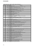
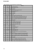
DIGITAL BOARD IC2601 MB91F155-3ES-X100 (MAIN SYSTEM CONTROLLER)
Pin No.
Pin Name
I/O
Description
1
DSP CLK
O
Serial data transfer clock signal output to the digital signal processor
2
DSP HDIN
O
Serial data output to the digital signal processor
3
1BST SEL
O
Boot strap signal output to the clock select
4
1XRST
O
System reset signal output to the digital signal processor “L”: reset
5
1PM
O
PLL initialize signal output to the digital signal processor
6
1GP9
I
Read ready signal input from the digital signal processor
7
1BST
O
Boot strap signal output to the digital signal processor
8
1HCS
O
Chip select signal output to the digital signal processor
9
VSS
—
Ground terminal
10
1HDOUT
I
Serial data input from the digital signal processor
11
1HACN
I
Acknowledge signal input from the digital signal processor
12
2XRST
O
System reset signal output to the digital signal processor “L”: reset
13
2PM
O
PLL initialize signal output to the digital signal processor
14
2GP3
I
Read ready signal input from the digital signal processor
15
2BST
O
Boot strap signal output to the digital signal processor
16
2HCS
O
Chip select signal output to the digital signal processor
17
2HDOUT
I
Serial data input from the digital signal processor
18
2HACN
I
Acknowledge signal input from the digital signal processor
19
2EXLOCK
O
PLL lock error signal and data error flag output to the digital sigal processor
20
DIR-XMODE
O
System reset signal output to the digital audio interface receiver “L”: reset
21
DIR-CKSEL
O
Output clock selection signal output to the digital audio interface receiver
22
DIR-CLK
O
Clock signal output to the digital audio interface receiver
23
DIR-CE
O
Chip enable signal output to the digital audio interface receiver
24
DIR-DO
I
Read data input from the digital audio interface receiver
25
DIR-DI
O
Write data output to the digital audio interface receiver
26
VSS
—
Ground terminal
27
VCC
—
Power supply terminal (+3.3V)
28
DIR-ERROR
I
PLL lock error signal and data error flag input from the digital audio interface receiver
29
DIR-DATAO
I
Audio serial data input from the digital audio interface receiver
30
DIR-XSTATE
I
Source clock selection monitor input from the digital audio interface receiver
31
TA_XCS
O
Chip select signal output to the lip sync adjust Not used
32
TA_SO
I
Serial data input from the lip sync adjust Not used
33
TA_XRST
O
Reset signal output to the lip sync adjust Not used
34
ADINT1
O
Reset signal output to the A/D converter
35
ADINT2
O
Reset signal output to the sub-2 system controller
36
D595OE
O
Output enable signal output to the TC74HC595AF
37
LAT1
O
Serial data latch pulse output to the TC74HC595AF
38
LAT2
O
Serial data latch pulse output to the TC74HC595AF
39
COM1CLK
O
Common clock signal output terminal
40
COM1DATA
O
Common data output terminal
41
COM2DATA
O
Common data output terminal
42
COM2CLK
O
Common data transfer clock signal output terminal
43
V595OE
O
Output enable signal output to the TC74HC595AF
44
VSS
—
Ground terminal
45
V595LAT
O
Serial data latch pulse output to the TC74HC595A


