


HCD-SLK1i/SLK2i
57
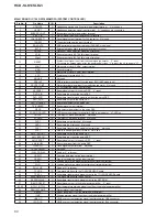
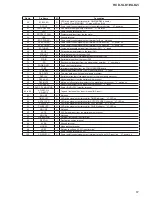
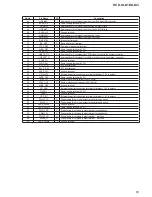
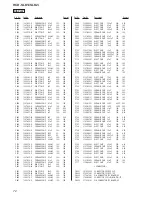
Pin No.
Pin Name
I/O
Description
1
USBA_ID
I
Not used
2
USBA_VBUS
I
VBUS (for USB connectior) detection signal input terminal
3
USB VDD3.3
-
Power supply terminal (+3.3V)
4
I/O
Two-way USB data (+) bus with the USB connector
5
USBA_D–
I/O
Two-way USB data (–) bus with the USB connector
6
USBA VSS3.3
-
Ground terminal
7
USBA txrtune
I
Reference voltage input terminal
8
USBA VSS3.3
-
Ground terminal
9
USBA VDD3.3
-
Power supply terminal (+3.3V)
10
USBB_ID
I
Not used
11
USBB_VBUS
I
VBUS (for iPod connectior) detection signal input terminal
12
USBB VDD3.3
-
Power supply terminal (+3.3V)
13
I/O
Two-way USB data (+) bus with the iPod connector
14
USBA_D–
I/O
Two-way USB data (–) bus with the iPod connector
15
USBB VSS
-
Ground terminal
16
USBB txrtune
I
Reference voltage input terminal
17
USBB VSS3.3C
-
Ground terminal
18
USBB VDD3.3
-
Power supply terminal (+3.3V)
19
PLL VDD3.3
-
Power supply terminal (+3.3V)
20
PLL VSS
-
Ground terminal
21 to 23
656D0 to 656D2
I
Digital video data input from the video D/A converter
24
VDD3.3
-
Power supply terminal (+3.3V)
25 to 27
656D3 to 656D5
I
Digital video data input from the video D/A converter
28
VDD1.2
-
Power supply terminal (+1.2V)
29, 30
656D6, 656D7
I
Digital video data input from the video D/A converter
31
DVSS
-
Ground terminal
32
iPod DET
I
iPod connection detection signal input terminal
33
iPod Acc Power
I
iPod accessory power detection signal input terminal
34
Card Vcc
OverCurrent DET
I
Card power over current detection signal input terminal
35
NC
-
Not used
36
SPI CS
O
Chip select signal output to the
fl
ash ROM
37
SPI HOLD
O
Hold signal output terminal Not used
38
SPI C/M1 D0
I/O
Serial data transfer clock signal output to the
fl
ash ROM
Two-way data bus with the SD-RAM
39
SPI D/M1 D1
I/O
Serial data output to the
fl
ash ROM
Two-way data bus with the SD-RAM
40
SPI Q/M1 D2
I/O
Serial data input from the
fl
ash ROM
Two-way data bus with the SD-RAM
41
SPI WP/M1 D3
I/O
Write protect signal output terminal Not used
Two-way data bus with the SD-RAM
42
VDD3.3
-
Power supply terminal (+3.3V)
43, 44
M1 D4, M1 D5
I/O
Two-way data bus with the SD-RAM
45
DVSS
-
Ground terminal
46, 47
M1 D6, M1 D7
I/O
Two-way data bus with the SD-RAM
48
M1DQM0
O
Data mask signal output to the SD-RAM
49 to 53
M1 D15, M1 D11
I/O
Two-way data bus with the SD-RAM
54
VDD3.3
-
Power supply terminal (+3.3V)
55 to 57
M1 D10 to M1 D8
I/O
Two-way data bus with the SD-RAM
58
M1DQM1
O
Data mask signal output to the SD-RAM
59
DVSS
-
Ground terminal
60
M1 CLKO
O
Clock signal output to the SD-RAM
61
M1 CKE
O
Clock enable signal output terminal Not used
62 to 69
M1 A12, M1 A11,
M1 A9 to M1 A4
O
Address signal output to the SD-RAM
70
VDD3.3
-
Power supply terminal (+3.3V)
71
M1 WE n
O
Write enable signal output to the SD-RAM
72
M1 CAS n
O
Column address signal output to the SD-RAM
73
M1 RAS n
O
Row address signal output to the SD-RAM
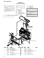
DISPLAY BOARD IC401 AML6226D (AUDIO DSP, DISPLAY CONTROLLER)


