


HCD-SLK1i/SLK2i
HCD-SLK1i/SLK2i
26
26
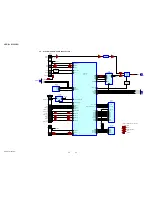
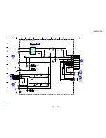
For Schematic Diagrams.
Note:
• All capacitors are in
μ
F unless otherwise noted. (p: pF) 50
WV or less are not indicated except for electrolytics and
tantalums.
• All resistors are in
Ω
and 1/4 W or less unless otherwise
speci
fi
ed.
•
f
: internal component.
•
C
: panel designation.
THIS NOTE IS COMMON FOR PRINTED WIRING BOARDS AND SCHEMATIC DIAGRAMS.
(In addition to this, the necessary note is printed in each block.)
•
A
: B+ Line.
•
B
: B– Line.
• Voltages and waveforms are dc with respect to ground
under no-signal conditions.
no mark : TUNER
• Voltages are taken with VOM (Input impedance 10 M
Ω
).
Voltage variations may be noted due to normal production
tolerances.
• Waveforms are taken with a oscilloscope.
Voltage variations may be noted due to normal production
tolerances.
• Circled numbers refer to waveforms.
• Signal path.
F
:
AUDIO
E
:
VIDEO
J
: DISC PLAY
f
:
TUNER
p
: USB
g
: iPod
l
: MEMORY CARD
i
: AUDIO IN
• Abbreviation
AR :
Argentina
model
BR
: Brazilian model
CH
: Chinese model
CND : Canadian model
E2
: 120 V AC area in E model
E3
: 240 V AC area in E model
E51
: Chilean and Peruvian models
EA
: Saudi Arabia model
KR
: Korean model
MX
: Mexican model
SP
: Singapore model
TH :
Thai
model
• The voltage and waveform of CSP (chip size package)
cannot be measured, becaise its lead layout is different
from that of conventional IC.
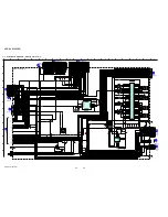
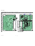
For Printed Wiring Boards.
Note:
•
X
: Parts extracted from the component side.
•
Y
: Parts extracted from the conductor side.
•
x
: Parts mounted on the conductor side.
•
f
: Internal component.
•
: Pattern from the side which enables seeing.
(The other layers' patterns are not indicated.)
• Indication of transistor.
C
B
These are omitted.
E
Q
B
These are omitted.
C E
Q
• Abbreviation
AR :
Argentina
model
BR
: Brazilian model
CH
: Chinese model
CND : Canadian model
E2
: 120 V AC area in E model
E3
: 240 V AC area in E model
E51
: Chilean and Peruvian models
EA
: Saudi Arabia model
KR
: Korean model
MX
: Mexican model
SP
: Singapore model
TH :
Thai
model
• Lead layouts
surface
CSP (Chip Size Package)
Lead layout of conventional IC
Caution:
Pattern face side:
(Conductor Side)
Parts face side:
(Component Side)
Parts on the pattern face side seen
from the pattern face are indicated.
Parts on the parts face side seen from
the parts face are indicated.
• DISPLAY board is multi-layer printed board. However, the
patterns of intermediate-layers have not been included in
this diagrams.
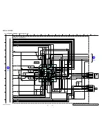
• Circuit Boards Location
Caution:
Pattern face side:
(SIDE B)
Parts face side:
(SIDE A)
Parts on the pattern face side seen
from the pattern face are indicated.
Parts on the parts face side seen from
the parts face are indicated.
Note:
The components identi
fi
ed by mark
0
or
dotted line with mark
0
are critical for safety.
Replace only with part number speci
fi
ed.
Note:
Les composants identi
fi
és par une marque
0
sont critiques pour la sécurité.
Ne les remplacer que par une piéce portant
le numéro spéci
fi
é.
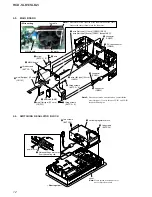
MS-214 board
LCD board
TOUCH PANEL board
JACK board
TERMINAL board
SWITCHING REGULATOR
KEY-RIGHT board
MAIN board
KEY-LEFT board
HP board
DISPLAY board
IP board
TUNER (FM/AM)


