DVP-LS500
3-13
3-14
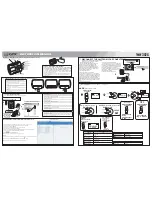
3-7. INTERFACE CONTROL BLOCK DIAGRAM
3
2
11
47
69
77
71
34
12
5
11
IC404
IF CON
IC408
RESET
IR
SEG 1 – 23
DIG 1 – 7
X401
8MHz
34
AD1
35
O/C
XIN
XOUT
1
VOUT
8
/RST
4
7
5
S803
S801
S805
S802
S816
1
CN801
REMOTE COMMANDER
RECEIVER
4
3
AF-98 BOARD (3/3)
(SEE PAGE 4-33)
ı
ı
ı
ı
05
1
AD1
O/C
IR
CN402
SW-384 BOARD
IC820
S809
VOUT
17
16
15
27
14
23
24
7
1
4
3
8
6
5
SYSTEM CONTROL
(SEE PAGE 3-8)
CN401
SC0
SI0
SO0
XIFBUSY
XIFCS
XFRRST
/SC
SO
SI
BUSY
/CS
/FRRST
/AMUTE
/VMUTE
SC0
SI0
SO0
XIFBUSY
XIFCS
XFRRST
AUDIO
(SEE PAGE 3-12)
VIDEO
(SEE PAGE 3-9)
A MUTE
VMUTE
(SEE PAGE 4-36)
ND401
VACUUM
FLUORESCENT
DISPLAY
3.4 Vp-p (8 MHz)
IC404
3