4-35
COVER
COVER
DSC-U30
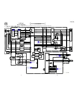
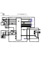
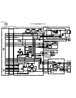
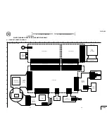
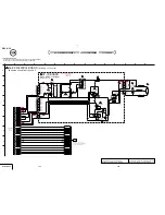
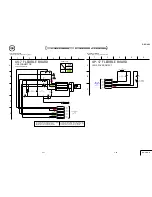
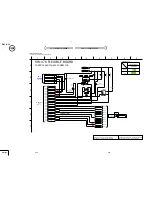
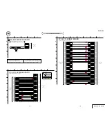
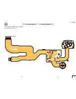
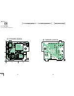
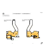
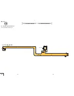
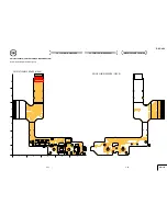
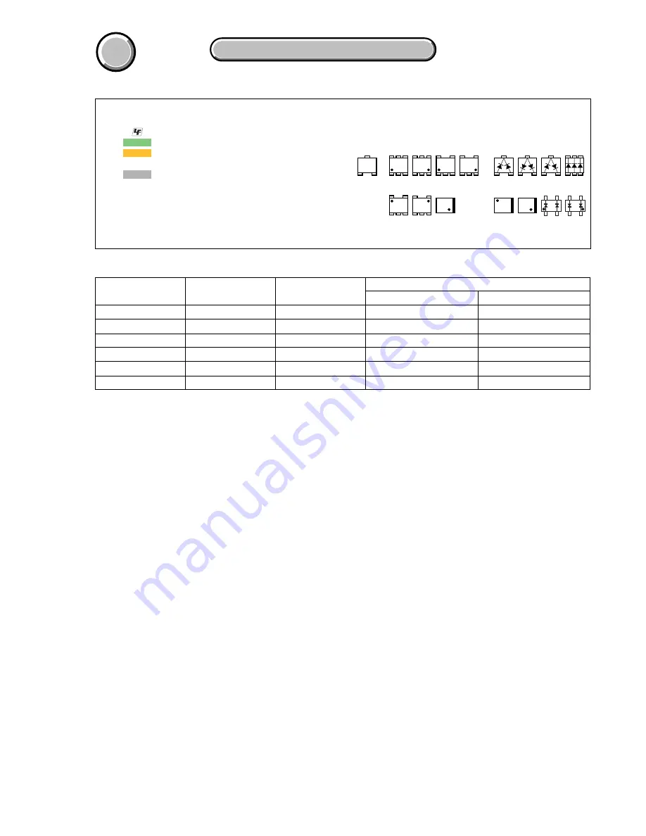
4-3. PRINTED WIRING BOARDS
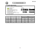
4-3. PRINTED WIRING BOARDS
•
: Uses unleaded solder.
•
: Circuit board
: Flexible board
Pattern from the side which enables seeing.
: pattern of the rear side
(The other layers’ patterns are not indicated)
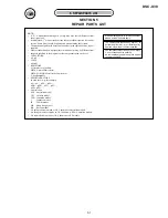
• Through hole is omitted.
• Circled numbers refer to waveforms.
• There are a few cases that the part printed on diagram
isn’t mounted in this model.
•
C
: panel designation
THIS NOTE IS COMMON FOR PRINTED WIRING BOARDS
2
1
3
2
1
3
2
1
3
3
4
5
2
1
1
2
3
6
5
4
E
B
C
3
1
5
5
2
4
6
1
2
3
5
4
4
3
1
2
1
2
4
3
3
1 2
4
5
5
3 4
1
2
3
4
2
1
1
2
4
3
4
6
2
5
3
1
1
2
4
3
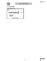
• Chip parts.
Transistor
Diode
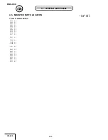
4-3. PRINTED WIRING BOARDS
Board Name
Parts Location
Waveforms
Pattern
Total Number of Layers
Layers Not Indicated
CD-425
4-60
4-57
3 layers
2 layers
SL-59
–
–
1 layer
–
ST-79
4-63
–
4 layers
2, 3 layers
US-7
–
–
3 layers
2 layers
OP-17
–
–
1 layer
–
SW-376
4-63
–
2 layers
–
Содержание Cyber-shot U DSC-U30
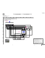
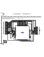
Страница 27: ...Schematic diagrams of the TY 20 PD 174 and DD 209 boards are not shown Pages from 4 11 to 4 24 are not shown ...
Страница 42: ...Waveforms of the TY 20 and PD 174 boards are not shown Pages 4 58 and 4 59 are not shown ...
Страница 44: ...Mounted parts location of the TY 20 PD 174 and DD 209 boards are not shown Pages 4 61 and 4 62 are not shown ...
Страница 57: ...DSC U30 76 Sony EMCS Co 2004J0500 1 2004 10 Published by DI Technical Support Section 9 876 263 31 ...

