26
These two outputs pass through low-pass filters CP801 and 802 respectively to remove harmonic component.
These CP801 and 802 are also used as directional couplers to detect a part of the power amplifier output for the
power control. The outputs of CP801 and 802 are entered to the front-end module CP702. This module switches
over the transmission, reception, and band, as mentioned previously. The signals entered to the CP702 are
outputted from the antenna via reversed route of received signals.
The signals detected in the CP801 and 802 are entered to the D803 and D802 respectively, and they are rectified
to become DC voltage components. These outputs are composed into one, and it is compared with APC signal
from base band in the operation amplifier IC801 to be the signal to control the CP803 so that the output voltage
can follow the APC signal.
(3) PLL Section
The PLL block consists of dual PLL (IC601) and VCO601 and VCO602. The VCO601 is for channel PLL and
generates thefollowing oscillation frequencies.
Transmission
1370.4 – 1439.6MHz 400kHz step
GSM band
Reception
1365.2 – 1399.8MHz 200kHz step
Transmission
1385.2 – 1459.8MHz 200kHz step
DCS band
Reception
1365.2 – 1439.8MHz 200kHz step
The output of VCO601 is entered to the FL601 and distributed to two outputs. One of these outputs returns to the
IC601, and another output is entered to the IC604. In the transmission of GSM band, the signal entered to the
IC604 is divided into two internally, and therefore the frequencies of every 400kHz step are used in this case only.
The VCO602 is for local PLL and generates the following oscillation frequencies.
Transmission : 975MHz
Reception :
880MHz
At the signal transmission, 975MHz is divided into five in the GSM band, or three in the DCS band in the IC604.
At the signal reception, 880MHz is always divided into two in the IC604.
Each VCO is provided with an external switching transistor so as to control the power supply.
(4) TCXO Section
The X601 is a VCTCXO module and it oscillates 13MHz reference signal. This oscillation frequency can be finely
adjusted by AFC signal from the DSP. The output signal of X601 is given to the IC601 as it is, and also buffered
in the Q602 and then supplied to the base band.
(5) Power Supply Section
The power supply voltage given from the battery side is supplied directly to the power amplifier module (CP803).
For other blocks, the power is supplied from the regulator ICs, IC501 and IC502.
The IC501 supplies 2.8V to the PLL block, while the IC502 supplies 2.8V to other blocks.
Содержание CMD-MZ5
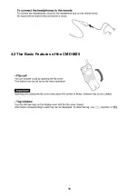
Страница 12: ...12 4 2 The Basic Features of the CMD MZ5 ...
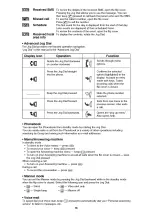
Страница 13: ...13 ...
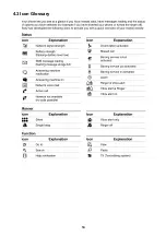
Страница 14: ...14 4 3 Icon Glossary ...
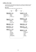
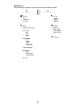
Страница 15: ...15 4 4 Menu Overview ...
Страница 16: ...16 ...
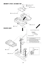
Страница 18: ...18 MEMORY STICK CONNECTOR BOARD ASSY ...
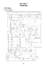
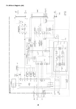
Страница 24: ...24 SECTION 7 DIAGRAMS 7 1 RF Block 7 1 1 Block Diagram ...
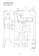
Страница 27: ...27 7 2 Base Band Block 7 2 1 Block Diagram 1 2 ...
Страница 28: ...28 7 2 2 Block Diagram 2 2 ...
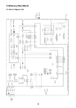
Страница 30: ...30 7 3 Memory Stick Block 7 3 1 Block Diagram 1 2 ...
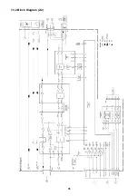
Страница 31: ...31 7 3 2 Block Diagram 2 2 ...
Страница 35: ...Sony Corporation Digital Telecommunication Company 9 870 403 01 2001 5 Published by After Sales Service ...

