25
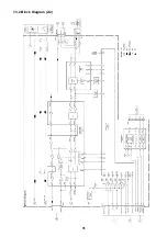
7.1.2 Operational Description
(1) Receiver Section
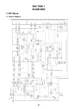
Radio signals received from the antenna located on the top of cabinet enter the RF connector of common
connector (CN401) provided at the bottom of cabinet.
After they are separated from the signals coming from external units by a mechanical switch, they enter the
antenna switch module (CP702). This module separates the signals transmitted/received to/from the antenna by
means of the switch, and also selects GSM or DCS band. The received signals are separated here into GSM side
and DCS side.
The received signals in the GSM band pass through the band-pass filter (SWF702) from CP702 to remove the
signals out of the receiving band. Then, the received signals are amplified in the low-noise amplifier using the
transistor (Q702).
Further, the band-pass filter (SWF704) removes unnecessary signals out of the band.
The SWF704 output signals are balanced signals. Thus, the signals from band-pass filter can be entered as
balanced signals to the subsequent RF IC IC604 having a balanced input system.
Similarly, the received signals in the DCS band pass through the band-pass filter (FL701) from CP702 to remove
the signals out of the receiving band. Then, the received signals are amplified in the low-noise amplifier using the
transistor (Q701), and further the band-pass filter (SWF703) removes unnecessary signals out of the band. Same
as in GSM band, the SWF703 output signals are also balanced signals, so that they can be entered to the IC604
as they are. FL701 is a dielectric filter, while SWF702 to SWF704 are all SAW filters.
To prevent characteristic deterioration due to bias point fluctuation at high temperature, the Q701 and Q702
detect current flowing in the transistors using signals at pins 37 to 39 of IC604 and perform the feedback control
so that the current flowing in the transistors is constant at all times.
Respective input signals in GSM and DCS bands entered to the IC604 are entered to the receiving mixer in the
IC604. They are mixed with local signals from VCO601 in the mixer and converted into IF signals in the 440MHz
band. The output of IF signals passes through the band-pass filter (SWF601) where unnecessary signals are
removed. The SWF601 output signals return to the IC604 again.
The SWF601 input/output signals are all balanced signals. The signals in the 440MHz band that returned to the
IC604 are adjusted to proper level signals by variable gain amplifier (PGC) in the IC604, and then they are
orthogonal-demodulated with 440MHz signal obtained by dividing the oscillation frequency 880MHz by two at the
signal reception from VCO602, and they become base band IQ signals in the IC604.
The received signals that became base band IQ signals pass through low-pass filter in the IC604 to remove
unnecessary signals, and then they are sent to the base band side.
The signals sent to the base band side are IQ signals having 1.4V DC offset.
(2) Transmitter Section
IQ signals transmitted from base band side are modulated into signals in the transmission IF frequency band by
an orthogonal modulator in the IC604. IQ signals must have DC offset voltage 1.575V typ. and signal amplitude
500mVp-p. The transmission IF frequency is 195MHz (975MHz/5) when the terminal is in GSM mode, or 325MHz
(975MHz/3) in DCS mode. By this modulation, local signals are generated by dividing the oscillation frequency
(975MHz) by an internal frequency divider (3/5 switching) at the signal transmission from VCO602.
The modulated signals outputted from orthogonal modulator pass through low-pass filter in the IC604, and then
they enter the phase comparator of the offset loop system modulator.
In the offset loop system modulation, the VCO having same oscillation frequency as transmission frequency is
assembled in the phase lock loop, and the reference frequency of this phase lock loop is used as transmission IF
frequency to adjust the phase shift of VCO to that of transmission IF frequency. As a result, the same effect as if
the phase modulation was applied to the transmission frequency can be attained.
Also, the transmission frequency can be selected simultaneously by using the output of VCO mixed down with the
frequency divided by VCO601 as a comparison frequency of the phase lock loop.
Unlike conventional mix up system, this offset loop system can reduce spurious signals generated in the mixer.
The output signals of offset loop are converted into the GMSK modulated signals by the power VCO, VCO801.
This VCO has two outputs of GSM band and DCS band, and the operation modes can be switched by signal
lines.
The output of VCO801 is already GMSK modulated waves of transmission frequency. The output of VCO801 in
the GSM band passes through the low-pass filter FL805 where harmonic component is attenuated. As the PA
module CP803 has only one input, this output is composed into one in the diplexer FL806. Also, a part of signals
returns to the IC604 for the input of phase lock loop. The output of FL806 enters the PA module CP803 via the
matching circuit. The CP803 is a power amplifier having dual bands, and which frequency is to be outputted is
switched over by the signal lines.
This power amplifier has output controllable terminals, so that the output voltage can be controlled according to
external voltage.
The CP803 generates two outputs, GSM and DCS.
Содержание CMD-MZ5
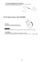
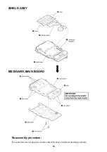
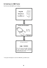
Страница 12: ...12 4 2 The Basic Features of the CMD MZ5 ...
Страница 13: ...13 ...
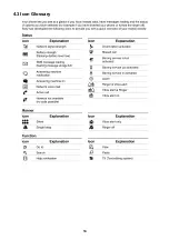
Страница 14: ...14 4 3 Icon Glossary ...
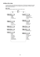
Страница 15: ...15 4 4 Menu Overview ...
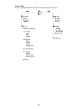
Страница 16: ...16 ...
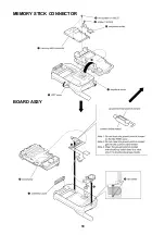
Страница 18: ...18 MEMORY STICK CONNECTOR BOARD ASSY ...
Страница 24: ...24 SECTION 7 DIAGRAMS 7 1 RF Block 7 1 1 Block Diagram ...
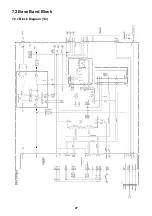
Страница 27: ...27 7 2 Base Band Block 7 2 1 Block Diagram 1 2 ...
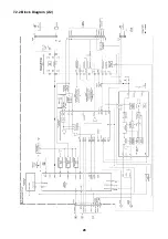
Страница 28: ...28 7 2 2 Block Diagram 2 2 ...
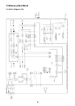
Страница 30: ...30 7 3 Memory Stick Block 7 3 1 Block Diagram 1 2 ...
Страница 31: ...31 7 3 2 Block Diagram 2 2 ...
Страница 35: ...Sony Corporation Digital Telecommunication Company 9 870 403 01 2001 5 Published by After Sales Service ...

