

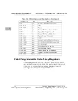
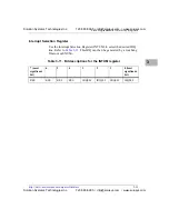


Field Programmable Gate Array Registers
http://www.motorola.com/computer/literature
3-7
3
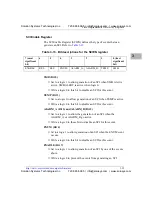
When a system management event occurs, the input causing the event
latches and remains latched until cleared by the system software. The
system management hardware notifies the system of the event depending
on the mode selected by the user. Refer to
.
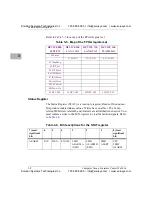
FPGA Register Descriptions
This section describes how to access the various FPGA register sets. The
bit description tables below show bits 0 through 7 on the top line and bit
functions on the second line.
You can access the FPGA registers by an index register at offset 05h from
the base address of the FPGA (0x5Dh). The data register is located at offset
07h (0x5Fh). Refer to
. To access an FPGA register, write to the
index register first and then read/write from the data register. The BIOS
sets the default FPGA Base address to 58h.
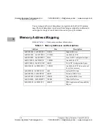
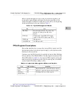
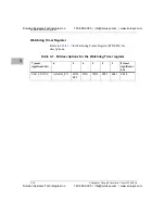
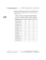
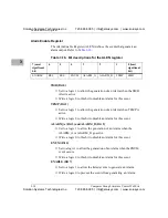
Table 3-3. System Management Modes
In:
an:
IRQ Mode
ISA interrupt generates - You can set the
interrupt by writing to the IRQ select
register.
SCI Mode
SCI generates - The FPGA’s SCI output
connects to the PIIX4 Therm input GPI8.
NMI Mode
NMI generates
ALARM Mode
ALARM generates
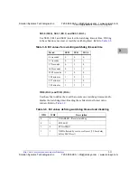
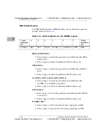
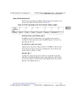
Table 3-4. Index and data register address and function
Port
Offset address
Function
Index
05h
Register Index Port - selects the device register
Data
07h
Data Port - read/write data to selected register
Watchdog
Strobe/Status
03h
Watchdog Strobe and Status register
Solution Systems Technologies Inc.
720-565-5995 | [email protected] | www.solusys.com
Solution Systems Technologies Inc.
720-565-5995 | [email protected] | www.solusys.com