SiRFatlasV
Hardware Design Guide
January, 2010
SiRF Design Guide
– Proprietary and Confidential
5
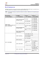
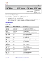
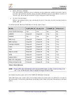
Working Mode
X_TEST_MODE[5:4]
Sub-Mode
X_TEST_MODE[3:2]
Feature 1
X_TEST_MODE[1]
Feature 0
X_TEST_MODE[0]
1’b1: Macro Test2
1’b0: MEM PHY
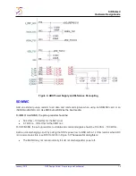
TEST
1’b1: Reserved
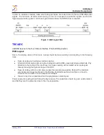
Table 1: Mode Configuration Pins
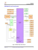
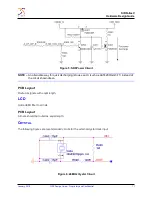
The following lists the configuration rules for different boot modes:
For SD/MMC boot mode, use the SD0 port.
For SLC NAND Flash/MLC and SD boot media, use UART1 to download the Nboot image. This
means that UART1 must be used as the debug port for the MLC/SD boot mode.
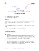
P
OWER
S
UPPLY
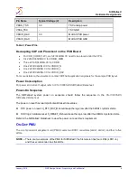
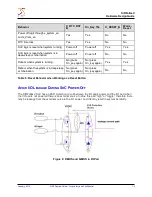
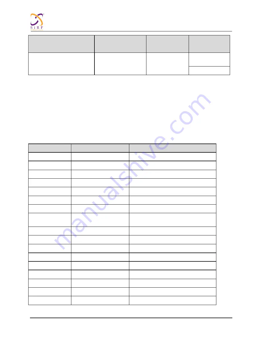
Power Pins
Pin Name
Typical Voltage (V)
Description
VDDIO_L
3.3/3.0/2.8/1.8
LCD related I/O pads power
VDDIO_N
3.3/3.0/2.8/1.8
NAND flash related I/O pads power
VDDIO
3.3/3.0/2.8
I/O pads power
VDDIO_MEM
1.8/2.5
The pad power of the memory interface
VDD_CORE
1.2
Main core digital power
GND
-
Main digital GND
VDDIO_RTC
3.3
RTC pad power
VDD_RTC
-
Internal LDO output, connect to bypass
cap
VDD_PLL0/1
1.2
PLL pad power
VSS_PLL0/1
-
PLL GND
VDDIO_OSC
3.3
OSC Pad power
VSSIO_OSC
-
OSC PAD GND
VDD_USB
1.2
USB core digital power
VDDA_USB
3.3
USB analog power
VSSA_USB
-
USB GND
VDD_TSC
1.2
TSC core digital power
VSS_TSC
-
TSC core GND