SiRFatlasV
Hardware Design Guide
January, 2010
SiRF Design Guide
– Proprietary and Confidential
8
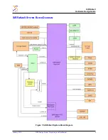
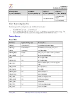
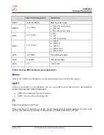
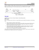
USP
All USP ports can support the DMA function which allows users to transmit large amounts of data at high
speed.
USP ports can simulate UART functions but do not support odd/even parity.
USP ports can simulate PCM or I
2
S (DSP mode), in this case X_TFS_0,1 itself can be used as a frame
sync pin.
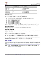
NAND
Add a pull-up resistor on the pin X_DF_WP_B since it is open drain.
DRAM
Refer to
CS-129773-UG SiRFatlasV DDR2/mDDR Hardware Design Guide
.
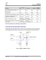
USB
Pay attention to the following when designing the USB module:
Add ESD devices to the DP/DN and ID pins.
Add an 820-Ohm resistor in series with the pin x_usb_vbus to prevent overvoltage.
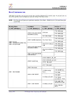
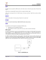
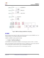
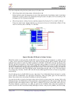
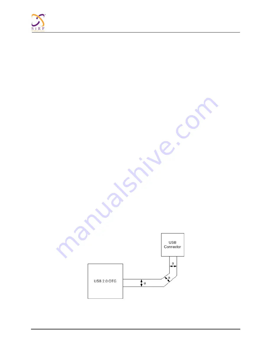
PCB Layout
The USB 2.0 specification requires that the USB DP/DN traces maintain a 90 Ohm differential impedance
(see paragraph 7.1.1.3 in USB specification Rev 2.0 for more details). A continuous ground plane is
required directly beneath the DP/DN traces and extending at least 5 times the spacing width to either side
of the DP/DN lines. Maintain the differential impedance close to 90 Ohm.
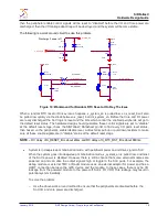
For different dielectric thicknesses, copper weight or board stack-ups, the trace width and spacing will
need to be recalculated. Keep the DP and DM lines symmetrical both in shape and length. Single-ended
impedance is not as critical as the differential impedance, a range of 42 Ohm to 78 Ohm is acceptable
(while the common mode impedance must be within the range of 21 Ohm to 39 Ohm).
Figure 2: USB DP/DN Route